Features: • Channel Select Input Over−Voltage Tolerant to 5.5 V• Fast Switching and Propagation Speeds• Break−Before−Make Circuitry• Low Power Dissipation: ICC = 2 A (Max) at TA = 25°C• Diode Protection Provided on Channel Select Input• Improve...
NLAS44599: Features: • Channel Select Input Over−Voltage Tolerant to 5.5 V• Fast Switching and Propagation Speeds• Break−Before−Make Circuitry• Low Power Dissipation: ...
SeekIC Buyer Protection PLUS - newly updated for 2013!
268 Transactions
All payment methods are secure and covered by SeekIC Buyer Protection PLUS.
US $.2 - .23 / Piece
Multiplexer Switch ICs 2:1 Mux/Demux Switch -55 to 125deg C
Symbol | Parameter | Value | Unit |
VCC | Positive DC Supply Voltage | -0.5 to +7.0 | V |
VIS | Analog Input Voltage (VNO or VCOM) | -0.5 VISVCC +0.5 | V |
VIN | Digital Select Input Voltage | -0.5 VI + 0.5 | V |
IIK | DC Current, Into or Out of Any Pin | ±50 | mA |
PD | Power Dissipation in Still Air QFN−16 TSSOP−16 |
800 450 |
mA |
TSTG | Storage Temperature Range | -65 to +150 | °C |
TL | Lead Temperature, 1 mm from Case for 10 Seconds | 260 | °C |
TJ | Junction Temperature Under Bias | +150 | °C |
MSL | Moisture Sensitivity | Level 1 | |
FR | Flammability Rating Oxygen Index: 28 to 34 | UL 94−V0 (0.125 in) | |
VESD | ESD Withstand Voltage Human Body Model (Note 1) Machine Model (Note 2) Charged Device Model (Note 3) |
2000 200 1000 |
V |
ILatchUp | LatchUp Performance Above VCC and Below GND at 85C (Note 5) | ±300 | mA |
JA | Thermal Resistance SOT- 353 (Note 1) SOT- 553 |
80 164 |
°C/W |
Maximum Ratings are those values beyond which damage to the device may occur. Exposure to these conditions or conditions beyond those indicated may adversely affect device reliability. Functional operation under absolute−maximum−rated conditions is not implied. Functional operation should be restricted to the Recommended Operating Conditions.
1. Tested to EIA/JESD22−A114−A.
2. Tested to EIA/JESD22−A115−A.
3. Tested to JESD22−C101−A.
4. Tested to EIA/JESD78.
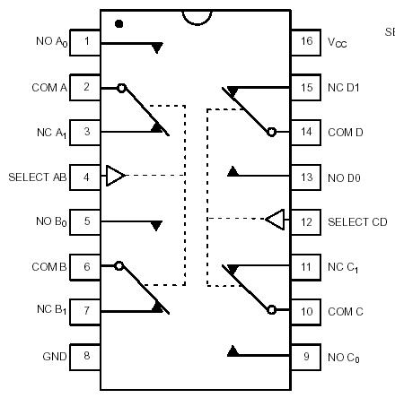
The NLAS44599 is an advanced dual−independent CMOS double pole−double throw (DPDT) analog switch fabricated with silicon gate CMOS technology. It achieves high speed propagation delays and low ON resistances while maintaining CMOS low power dissipation. This DPDT controls analog and digital voltages that may vary across the full power−supply range (from VCC to GND).
NLAS44599 has been designed so the ON resistance (RON) is much lower and more linear over input voltage than RON of typical CMOS analog switches.
The channel select input is compatible with standard CMOS outputs. The channel select input structure of NLAS44599 provides protection when voltages between 0 V and 5.5 V are applied, regardless of the supply voltage. This input structure helps prevent device destruction caused by supply voltage − input/output voltage mismatch, battery backup, hot insertion, etc.
The NLAS44599 can also be used as a quad 2−to−1 multiplexer− demultiplexer analog switch with two Select pins that each controls two multiplexer−demultiplexers.