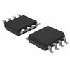
NLAS323

Features: • On Resistance is 20 Typical at 5.0 V• Matching is < 1.0 Between Sections• 2.0 to 6.0 V Operating Range• Ultra Low < 5.0 pC Charge Injection• Ultra Low Leakage < 1.0 nA at 5.0 V, 25• Wide Bandwidth > 200 MHz, −3.0 dB• 2000 V ...

product image

NLAS323 Picture
SeekIC No. : 004434744 Detail

NLAS323: Features: • On Resistance is 20 Typical at 5.0 V• Matching is < 1.0 Between Sections• 2.0 to 6.0 V Operating Range• Ultra Low < 5.0 pC Charge Injection• Ultra L...

floor Price/Ceiling Price

Part Number:
NLAS323
Supply Ability:
5000

Price Break

  • Qty
  • 1~5000
  • Unit Price
  • Negotiable
  • Processing time
  • 15 Days
Total Cost: $ 0.00

SeekIC Buyer Protection PLUS - newly updated for 2013!

  • Escrow Protection.
  • Guaranteed refunds.
  • Secure payments.
  • Learn more >>

Month Sales

268 Transactions

Rating

evaluate  (4.8 stars)

Upload time: 2024/11/23

Payment Methods

All payment methods are secure and covered by SeekIC Buyer Protection PLUS.

Notice: When you place an order, your payment is made to SeekIC and not to your seller. SeekIC only pays the seller after confirming you have received your order. We will also never share your payment details with your seller.
Product Details

Description


Features:

• On Resistance is 20 Typical at 5.0 V
• Matching is < 1.0 Between Sections
• 2.0 to 6.0 V Operating Range
• Ultra Low < 5.0 pC Charge Injection
• Ultra Low Leakage < 1.0 nA at 5.0 V, 25
• Wide Bandwidth > 200 MHz, −3.0 dB
• 2000 V ESD (Human Body Model)
• Ron Flatness ±6.0 at 5.0 V
• US8 Package
• Independent, Positive Enable
• Pb−Free Package is Available*


Pinout

  Connection Diagram


Specifications

Symbol Parameter Value Unit
VCC Positive DC Supply Voltage -0.5 to +7.0 V
VI Analog Input Voltage (VNO or VCOM) -0.5 to +7.0 V
VO DC Output Voltage -0.5 to +7.0 V
IIK DC Input Diode Current VI < GND -50 mA
IOK DC Output Diode Current VO < GND -50 mA
IO DC Output Sink Current ±50 mA
ICC DC Supply Current per Supply Pin ±100 mA
IGND DC Ground Current per Ground Pin ±100 mA
TSTG Storage Temperature Range -65 to +150 °C
TL Lead Temperature, 1 mm from Case for 10 Seconds 260 °C
TJ Junction Temperature under Bias +150 °C
JA Thermal Resistance (Note 1) 250 °C/W
PD Power Dissipation in Still Air at 85°C 250

mW
MSL Moisture Sensitivity Level 1  
FR Flammability Rating Oxygen Index: 28 to 34 UL 94?V0 (0.125 in)  
VESD ESD Withstand Voltage Human Body Model (Note 2)
Machine Model (Note 3)
Charged Device Model (Note 4)
> 2000
> 150
N/A
V

Maximum Ratings are those values beyond which damage to the device may occur. Exposure to these conditions or conditions beyond those indicated may adversely affect device reliability. Functional operation under absolute maximum−rated conditions is not implied. Functional operation should be restricted to the Recommended Operating Conditions.
1. Measured with minimum pad spacing on an FR4 board, using 10 mm−by−1 inch, 2−ounce copper trace with no air flow.
2. Tested to EIA/JESD22−A114−A.
3. Tested to EIA/JESD22−A115−A.
4. Tested to JESD22−C101−A.


Description

The NLAS323 is a dual SPST (Single Pole, Single Throw) switch, similar to 1/2 a standard 4066. The device permits the independent selection of 2 analog/digital signals. Available in the US8 package.

The use of advanced 0.6 micron CMOS process, NLAS323 improves the RON resistance considerably compared to older higher voltage technologies.


Customers Who Bought This Item Also Bought

Margin,quality,low-cost products with low minimum orders. Secure your online payments with SeekIC Buyer Protection.
Circuit Protection
Crystals and Oscillators
Programmers, Development Systems
Motors, Solenoids, Driver Boards/Modules
Optoelectronics
Integrated Circuits (ICs)
View more