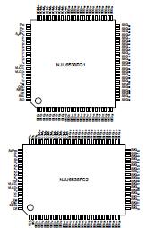
Features: · Direct Correspondence between Display Data RAM and LCD Pixel
· Display Data RAM : 650-bits
· LCD Drivers : 65-seg, 10-com
· Serial interface (SIO, SCL, CS)
· Programmable Duty Ratio
1/8 Duty 7-common x 65-segment + 1-icon common
1/9 Duty 7-common x 65-segment + 2-icon common
1/10Duty 7-common x 65-segment + 3-icon common
· Bias Ratio 1/4 bias
· 25-key scan Function (5 x 5 matrix)
Needless for anti-reverse current diodes in key scan
· general Output Ports with 128-steps PWM output (possible LED driving) maximum 4-ports
· Useful Instruction Set
Display ON/OFF, Page Address Set, Column Address Set, Display Data write, ADC Select, Inverse Display ON/OFF, whole display ON/OFF, Reset, EVR Register Set, Duty Select, Power Save mode set, General Output Port PWM phase / frequency set, General Output Port PWM data set, General Output Port / Key scan output select
· Bleeder Resistance On-chip
· Software Contrast Control (16 steps)
· Operating Voltage
Logic Operating Voltage 2.7 to 5.5V
LCD Driving Voltage 5.0 to 10.0V
· Package Outline QFP100-G1
QFP100-C2
· C-MOS Technology (Substrate: P)
Pinout Specifications
| PARAMETER |
SYMBOL |
CONDITIONS |
RATINGS |
UNIT |
| Supply voltage |
VDD max |
VDD terminal |
-0.3 to +7.0 |
V |
| VLCD max |
VLCD1 terminal |
-0.3 to +11.0 |
| Input terminal voltage |
VIN1 |
OSC, K0 to K4,CE, SCL, SIO terminal |
-0.3 to VDD+0.3 |
V |
| VIN2 |
VLCD2, V0 to V2 terminal |
-0.3 to VLCD+0.3 |
| Output terminal voltage |
VOUT1 |
SIO terminal |
-0.3 to +6.0 |
V |
| VOUT2 |
OSC, SEG1 to SEG65,COM1 to COM10,
S1 to S4, Po0 to Po2, Po3 /S0 terminal |
-0.3 to VDD+0.3 |
| Power dissipation |
Pdmax |
Ta=25°C QFP100-C2 |
1000 |
mW |
| Ta=25°C QFP100-C1 |
700 |
| Storage temperature |
Tstg |
- |
-55 to +125 |
|
| Operating temperature |
Topr |
- |
-40 to +85 |
|
Note 1) All voltage values are specified as VSS=0V.
Note 2) If the LSI are used on condition beyond the absolute maximum rating, the LSI may be destroyed. Using LSI within electrical characteristics is strongly recommended for normal operation. Use beyond the erectric characteristics conditions will cause malfunction and poor reliability.
Note 3) Decoupling capacitor should be connected between VDD and VSS due to the stabilized operation forthe voltage converter.
DescriptionThe NJU6538 is a 10-common x 65-segment bitmap LCD
driver to display graphics or characters.
NJU6538 contains 650 bits display data RAM, microprocessor interface circuit, common and segment drivers, key scan circuit, and general output ports.
An image data of NJU6538 from MPU through the serial interface is stored into the 650 bits internal displayed on the LCD panel through the commons and segments drivers.
The NJU6538 displays 10 x 65 dots graphics or 11-character 1-line by 5 x 7 dots character + 3 x 65 dots icons. It contains key scan circuit transmitting the 25-keys maximum (5 x 5 = 25) to MPU.
Also NJU6538 provides 4 general purpose output ports with PWM output function maximum to drive LEDs or others directly.
Furthermore, the NJU6538 can select a LCD driving voltage out of 16 steps voltage by the instruction adjust the display contrast of LCD panel.

 NJU6538 Data Sheet


