Features: • Operates from ±5V to ±18V supplies• Hold leakage current 6pA @ TJ = 25°C• Less than 4ms acquisition time• TTL, PMOS, CMOS compatible logic input• 0.5mV typical hold step at CH=0.01mF• Low input offset: 1MV (typical)• 0.002% gain accuracy with R...
NE5537: Features: • Operates from ±5V to ±18V supplies• Hold leakage current 6pA @ TJ = 25°C• Less than 4ms acquisition time• TTL, PMOS, CMOS compatible logic input• 0.5mV typi...
SeekIC Buyer Protection PLUS - newly updated for 2013!
268 Transactions
All payment methods are secure and covered by SeekIC Buyer Protection PLUS.
Features: • High output power : Pout = 30.0 dBm TYP. (VDS = 4.8 V, IDset = 200 mA, f = 1.9 G...
SYMBOL | PARAMETER |
RATING |
UNIT |
VS | Voltage supply |
±18 |
V |
PD | Maximum power dissipation TA=25°C (still-air)1 | ||
N package |
1160 |
mW | |
D package |
1090 |
mW | |
FE package |
780 |
mW | |
TA | Operating ambient temperature range | ||
SE5537 |
-55 to +125 |
°C | |
NE5537 |
0 to +70 |
°C | |
TSTG | Storage temperature range |
-65 to +150 |
°C |
VIN | Input voltage |
Equal to supply voltage |
|
Logic to logic reference differential voltage2 |
+7, -30 |
V | |
Output short circuit duration |
Indefinite |
||
Hold capacitor short circuit duration |
10 |
s | |
TSOLD | Lead soldering temperature (10sec max) |
300 |
°C |
NOTES:
1. Derate above 25°C at the following rates:
FE package at 6.2mW/°C
N package at 9.3mW/°C
D package at 8.3mW/°C
2. Although the differential voltage may not exceed the limits given, the common-mode voltage on the logic pins may be equal to the supply voltages without causing damage to the circuit. For proper logic operation, however, one of the logic pins must always be at least 2V below the positive supply and 3V above the negative supply.
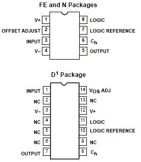
The NE5537 monolithic sample-and-hold amplifier combines the best features of ion-implanted JFETs with bipolar devices to obtain high accuracy, fast acquisition time, and low droop rate. NE5537 is pin-compatible with the LF198, and features superior performance in droop rate and output drive capability. The circuit shown in Figure 1 contains two operational amplifiers which function as a unity gain amplifier in the sample mode. The first amplifier has bipolar input transistors which give the system a low offset voltage. The second amplifier has JFET input transistors to achieve low leakage current from the hold capacitor. A unique circuit design for leakage current cancellation using current mirrors gives the NE5537 a low droop rate at higher temperature. The output stage has the capability to drive a 2kW load. The logic input is compatible with TTL, PMOS or CMOS logic. The differential logic threshold is 1.4V with the sample mode occurring when the logic input is high. NE5537 is available in 8-lead TO-5, 8-pin plastic DIP packages, and 14-pin SO packages.