Gate-Source Breakdown Voltage
: +/- 20 V
Mounting Style
: SMD/SMT
Packaging
: Reel
Maximum Operating Temperature
: + 150 C
Transistor Polarity
: N and P-Channel
Configuration
: Dual Dual Drain
Resistance Drain-Source RDS (on)
: 0.08 Ohms
Package / Case
: SOIC-8 Narrow
Drain-Source Breakdown Voltage
: +/- 30 V
Continuous Drain Current
: 3.7 A, - 2.9 A
Features: `N-Channel 3.7A, 30V, RDS(ON)=0.08 @ VGS=10V. P-Channel -2.9A, -30V, RDS(ON)=0.13 @ VGS=-10V.
`High density cell design or extremely low RDS(ON).
`High power and current handling capability in a widely used surface mount package.
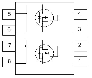
`Dual (N & P-Channel) MOSFET in surface mount package.Pinout Specifications
|
Symbol |
Parameter |
N-Channel |
P-Channel |
Units |
|
VDSS
VGSS |
Drain-Source Voltage
Gate-Source Voltage |
30
± 20
± 3.7
± 15 |
-30
± 20
± 2.9
± 10 |
V
V
A
W
°C |
|
ID |
Drain Current Continuous Pulsed |
(Note 1a) |
|
PD |
Power Dissipation for Dual Operation |
2
1.6
1
0.9
-55 to 150 |
| Power Dissipation for Single Operation |
(Note 1a)
(Note 1b)
(Note 1c) |
| TJ,TSTG |
Operating and Storage Junction Temperature Range |
THERMAL CHARACTERISTICS
RJA
RJC |
Thermal Resistance, Junction-to-Ambient
Thermal Resistance, Junction-to-Case |
(Note 1a)
(Note 1) |
78
40 |
°C/W
°C/W |
</TBO
DescriptionThese dual N- and P-channel enhancement mode power field effect transistors NDS9952A are produced using Fairchild's proprietary, high cell density, DMOS technology. This very high density process is especially tailored to minimize on-state resistance, provide superior switching performance, and withstand high energy pulses in the avalanche and commutation modes. NDS9952A is particularly suited for low voltage applications such as notebook computer power management and other battery powered circuits where fast switching, low in-line power loss, and resistance to transients are needed.
Parameters: | Technical/Catalog Information | NDS9952A |
| Vendor | Fairchild Semiconductor (VA) |
| Category | Discrete Semiconductor Products |
| Mounting Type | Surface Mount |
| FET Polarity | N and P-Channel |
| Drain to Source Voltage (Vdss) | 30V |
| Current - Continuous Drain (Id) @ 25° C | 3.7A, 2.9A |
| Rds On (Max) @ Id, Vgs | 80 mOhm @ 1A, 10V |
| Input Capacitance (Ciss) @ Vds | 320pF @ 10V |
| Power - Max | 900mW |
| Packaging | Cut Tape (CT) |
| Gate Charge (Qg) @ Vgs | 25nC @ 10V |
| Package / Case | SO-8 |
| FET Feature | Logic Level Gate |
| Lead Free Status | Lead Free |
| RoHS Status | RoHS Compliant |
| Other Names | NDS9952A
NDS9952A
NDS9952ACT ND
NDS9952ACTND
NDS9952ACT
|

 NDS9952A Data Sheet


