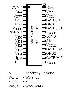
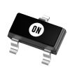
Features: • Enhanced V2 Control Method with Internal Ramp• Internal PWM Ramp• Fast−Feedback Directly from VCORE• VRM 9.X DAC with 1.0% Accuracy• Adjustable Output Voltage Positioning• 4 On−Board Gate Drivers• 200 kHz to 800 kHz Operation Set by...
NCP5332A: Features: • Enhanced V2 Control Method with Internal Ramp• Internal PWM Ramp• Fast−Feedback Directly from VCORE• VRM 9.X DAC with 1.0% Accuracy• Adjustable Output...
SeekIC Buyer Protection PLUS - newly updated for 2013!
268 Transactions
All payment methods are secure and covered by SeekIC Buyer Protection PLUS.
Features: • 50 Vrms Output Noise Without Use of Bypass Capacitor• Low Dropout Voltage ...
Rating |
VALUE |
SYMBOL |
Operating Junction Temperature |
150 |
°C |
Lead Temperature Soldering: Reflow: (SMD styles only) (Note 1) |
230 peak |
°C peak °C |
Package Thermal Resistance: Junction−to−Case, RqJC Junction−to−Ambient, RqJA |
15 75 |
°C |
Storage Temperature Range |
52
|
°C/W
|
ESD Susceptibility: Human Body Model Machine Model |
2.0
200 |
kV
|
JEDEC Moisture Sensitivity |
Level 2
|
-
|
The NCP5332A is a second−generation, two−phase step down controller which incorporates all control functions required to power high performance processors and high current power supplies. Proprietary multi−phase architecture guarantees balanced load current distribution and reduces overall solution cost in high current applications. Enhanced V2] control architecture provides the fastest possible transient response, excellent overall regulation, and ease of use.
The NCP5332A is a second−generation PWM controller because it optimizes transient response by combining traditional Enhanced V2 with an internal PWM ramp and fast−feedback directly from VCORE to the internal PWM comparator. These enhancements provide greater design flexibility, facilitate use and reduce output voltage jitter. The NCP5332A multi−phase architecture reduces output voltage and input current ripple, allowing for a significant reduction in filter size and inductor values with a corresponding increase in inductor current slew rate. This approach allows a considerable reduction in input and output capacitor requirements, as well as reducing overall solution size and cost.