NCP5201

Features: • Incorporates VDDQ, VTT Regulators• Internal Switching Standby Regulator for VDDQ• All External Power MOSFETs Are N−Channel• Adjustable VDDQ• VTT Tracks VDDQ/2• Fixed Switching Frequency of 250 kHz for VDDQ in Normal Mode• Doubled Switchin...

product image

NCP5201 Picture
SeekIC No. : 004433029 Detail

NCP5201: Features: • Incorporates VDDQ, VTT Regulators• Internal Switching Standby Regulator for VDDQ• All External Power MOSFETs Are N−Channel• Adjustable VDDQ• VTT Track...

floor Price/Ceiling Price

Part Number:
NCP5201
Supply Ability:
5000

Price Break

  • Qty
  • 1~5000
  • Unit Price
  • Negotiable
  • Processing time
  • 15 Days
Total Cost: $ 0.00

SeekIC Buyer Protection PLUS - newly updated for 2013!

  • Escrow Protection.
  • Guaranteed refunds.
  • Secure payments.
  • Learn more >>

Month Sales

268 Transactions

Rating

evaluate  (4.8 stars)

Upload time: 2025/1/9

Payment Methods

All payment methods are secure and covered by SeekIC Buyer Protection PLUS.

Notice: When you place an order, your payment is made to SeekIC and not to your seller. SeekIC only pays the seller after confirming you have received your order. We will also never share your payment details with your seller.
Product Details

Description


Features:

• Incorporates VDDQ, VTT Regulators
• Internal Switching Standby Regulator for VDDQ
• All External Power MOSFETs Are N−Channel
• Adjustable VDDQ
• VTT Tracks VDDQ/2
• Fixed Switching Frequency of 250 kHz for VDDQ in Normal Mode
• Doubled Switching Frequency (500 kHz) for Standby Mode
• Soft−Start Protection for VDDQ
• Undervoltage Monitor
• Short−Circuit Protection for Both VDDQ and VTT Outputs
• Housed in a space saving 5 × 6 QFN−18


Application

• DDR Termination Voltage
• Active Termination Busses (SSTL−2, SSTL−3)


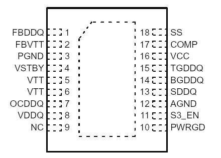
Pinout

  Connection Diagram


Specifications

Rating Symbol Value Unit
Power Supply Voltage (Pin 4) to PGND (Pin 3) and GND (Pin 12) VSTBY −0.3, 6.0 V
Power Supply Voltage, VCC (Pin 16) to PGND (Pin 3) and GND (Pin 12) VCC −0.3, 14 V
Gate Drive Voltage (Pins 14, 15) Vg −0.3 DC,
−4.0 for < 1.0 s; 14
V
Input/Output Pins (Pins 1, 2, 5−11, 13, 17−18) VIO −0.3, 6.0 V
Package Thermal Resistance
Junction−to−Ambient
RJA 35 °C/W
Operating Junction Temperature Range TJ 0 to +150 °C
Operating Ambient Temperature Range TA 0 to +70 °C
Storage Temperature Range Tstg −55 to +150 °C
Moisture Sensitivity Level MSL 2 °C

Maximum ratings are those values beyond which device damage can occur. Maximum ratings applied to the device are individual stress limit values (not normal operating conditions) and are not valid simultaneously. If these limits are exceeded, device functional operation is not implied, damage may occur and reliability may be affected.
1. This device series contains ESD protection and exceeds the following tests: Human Body Model (HBM) 3 2.0 kV per JEDEC Standard JESD22−A114 except Pin 15 which is 3 1.5 kV. Machine Model (MM) 3 200 V per JEDEC Standard JESD22−A115 except Pin 14 which is 3 100 V.
2. Latchup Current Maximum Rating: 3 150 mA per JEDEC Standard JESD78.


Description

The NCP5201 Dual DDR Power Controller is specifically designed as a total power solution for a high current DDR memory system. This IC combines the efficiency of a PWM controller for the VDDQ supply with the simplicity of a linear regulator for the VTT memory termination voltage. The secondary regulator (VTT) is designed to automatically track at half the primary regulator voltage (VDDQ). An internal power good voltage monitor tracks both VDDQ and VTT outputs and notifies the user in the event of a fault on either output. Protective features include soft−start circuitry and undervoltage monitoring of VCC and VSTBY. The IC of the NCP5201 is packaged in a 5 × 6 QFN−18.


Customers Who Bought This Item Also Bought

Margin,quality,low-cost products with low minimum orders. Secure your online payments with SeekIC Buyer Protection.
Sensors, Transducers
Optoelectronics
Isolators
Discrete Semiconductor Products
View more