NBSG72A

Features: • Maximum Input Clock Frequency > 7 GHz Typical• Maximum Input Data Rate > 7 Gb/s Typical• 200 ps Typical Propagation Delay (OLS = FLOAT)• 55/45 ps Typical Rise/Fall Times (OLS = FLOAT)• Selectable Swing PECL Output with Operating Range:VCC = 2.375 V t...

product image

NBSG72A Picture
SeekIC No. : 004432751 Detail

NBSG72A: Features: • Maximum Input Clock Frequency > 7 GHz Typical• Maximum Input Data Rate > 7 Gb/s Typical• 200 ps Typical Propagation Delay (OLS = FLOAT)• 55/45 ps Typical Ri...

floor Price/Ceiling Price

Part Number:
NBSG72A
Supply Ability:
5000

Price Break

  • Qty
  • 1~5000
  • Unit Price
  • Negotiable
  • Processing time
  • 15 Days
Total Cost: $ 0.00

SeekIC Buyer Protection PLUS - newly updated for 2013!

  • Escrow Protection.
  • Guaranteed refunds.
  • Secure payments.
  • Learn more >>

Month Sales

268 Transactions

Rating

evaluate  (4.8 stars)

Upload time: 2025/1/9

Payment Methods

All payment methods are secure and covered by SeekIC Buyer Protection PLUS.

Notice: When you place an order, your payment is made to SeekIC and not to your seller. SeekIC only pays the seller after confirming you have received your order. We will also never share your payment details with your seller.
Product Details

Description


Features:

• Maximum Input Clock Frequency > 7 GHz Typical
• Maximum Input Data Rate > 7 Gb/s Typical
• 200 ps Typical Propagation Delay (OLS = FLOAT)
• 55/45 ps Typical Rise/Fall Times (OLS = FLOAT)
• Selectable Swing PECL Output with Operating Range:VCC = 2.375 V to 3.465 V with VEE = 0 V
• Selectable Swing NECL Output with NECL Inputs with Operating Range:
    VCC = 0 V with VEE = −2.375 V to −3.465 V
• Selectable Output Levels (0 mV, 200 mV, 400 mV, 600 mV or 800 mV Peak−to−Peak Output)
• 50  Internal Input Termination Resistors
• Single−Ended LVECL or LVCMOS/LVTTL Select Inputs (SELA, SELB)
• Pb−Free Package is Available


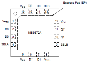
Pinout

  Connection Diagram


Specifications

Symbol
Parameter Condition 1 Condition 2
Rating
Units
VCC
Positive Power Supply VEE = 0 V  
3.6
V
VEE
Negative Power Supply VCC = 0 V  
-3.6
V
VI
Positive Input
Negative Input
VEE = 0 V
VCC = 0 V
VI VCC
VI VEE
3.6
-3.6
V
V
VINPP
Differential Input Voltage |DX - DX | VCC - VEE 2.8 V
VCC - VEE < 2.8 V
 
2.8
|VCC - VEE|
V
V
Iout
Output Current Continuous
Surge
 
25
50
mA
mA
IIN
Input Current Through RT (50 Resistor) Static
Surge
 

 80
 45

 mA
 mA

TA
Operating Temperature Range    
-40 to +85
Tstg
Storage Temperature Range    
-65 to +150
JA
Thermal Resistance (Junction-to-Ambient)
(Note 2)
0 LFPM
500 LFPM
QFN−16
QFN−16
42
35
/W
/W
/W
/W
JC
Thermal Resistance (Junction-to-Case) (Note 2) QFN−16
4
/W
Tsol
Wave Solder < 15 Sec  
225


Maximum ratings are those values beyond which device damage can occur. Maximum ratings applied to the device are individual stress limit values (not normal operating conditions) and are not valid simultaneously. If these limits are exceeded, device  unctional operation is not implied, damage may occur and reliability may be affected.
2. JEDEC standard multilayer board − 1S2P (1 signal, 2 power).


Description

The NBSG72A is a high−bandwidth fully differential 2 X 2 crosspoint switch with Output Level Select (OLS) capabilities. This is a part of the GigaComm] family of high performance Silicon Germanium products. The NBSG72A is housed in a low profile 3 X 3 mm  16−pin QFN package. Differential inputs incorporate internal 50  termination resistors and accept NECL (Negative ECL), PECL (Positive ECL), LVCMOS/LVTTL, CML, or LVDS. The OLS input is used to program the peak−to−peak output amplitude between 0 mV and 800 mV in five discrete steps. The SELECT inputs are single−ended and can be driven with either LVECL or LVCMOS/LVTTL input levels.


Customers Who Bought This Item Also Bought

Margin,quality,low-cost products with low minimum orders. Secure your online payments with SeekIC Buyer Protection.
Cables, Wires
Prototyping Products
DE1
Memory Cards, Modules
Power Supplies - External/Internal (Off-Board)
Static Control, ESD, Clean Room Products
Undefined Category
View more