NB6L239

Features: • Maximum Clock Input Frequency, 3.0 GHz• Input Compatibility with LVDS/LVPECL/CML/HSTL• Rise/Fall Time 70 ps Typical• < 10 ps Typical Output−to−Output Skew• Ex. 622 MHz Input Generates 38.8 MHz to 622 MHz Outputs• Internal 50  Terminat...

product image

NB6L239 Picture
SeekIC No. : 004432720 Detail

NB6L239: Features: • Maximum Clock Input Frequency, 3.0 GHz• Input Compatibility with LVDS/LVPECL/CML/HSTL• Rise/Fall Time 70 ps Typical• < 10 ps Typical Output−to−Outp...

floor Price/Ceiling Price

Part Number:
NB6L239
Supply Ability:
5000

Price Break

  • Qty
  • 1~5000
  • Unit Price
  • Negotiable
  • Processing time
  • 15 Days
Total Cost: $ 0.00

SeekIC Buyer Protection PLUS - newly updated for 2013!

  • Escrow Protection.
  • Guaranteed refunds.
  • Secure payments.
  • Learn more >>

Month Sales

268 Transactions

Rating

evaluate  (4.8 stars)

Upload time: 2024/11/22

Payment Methods

All payment methods are secure and covered by SeekIC Buyer Protection PLUS.

Notice: When you place an order, your payment is made to SeekIC and not to your seller. SeekIC only pays the seller after confirming you have received your order. We will also never share your payment details with your seller.
Product Details

Description


Features:

• Maximum Clock Input Frequency, 3.0 GHz
• Input Compatibility with LVDS/LVPECL/CML/HSTL
• Rise/Fall Time 70 ps Typical
• < 10 ps Typical Output−to−Output Skew
• Ex. 622 MHz Input Generates 38.8 MHz to 622 MHz Outputs
• Internal 50  Termination Provided
• Random Clock Jitter < 1 ps RMS
• Divide−by−1 Edge of QA Aligned to QB Divided Output
• Operating Range: VCC = 2.375 V to 3.465 V with VEE = 0 V
• Master Reset for Synchronization of Multiple Chips
• VBBAC Reference Output
• Synchronous Output Enable/Disable


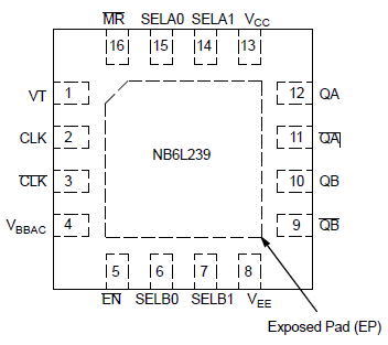
Pinout

  Connection Diagram


Specifications

Symbol
Parameter
Condition 1
Condition 2
Rating
Units
VCC
Positive Mode Power Supply VEE = 0 V  
3.6
V
VI
Input Voltage VEE = 0 V VEE VI VCC
3.6
V
Iout
Output Current Continuous
Surge
 
50
100
mA
mA
IBB
VBBAC Sink/Source    
± 0.5
mA
TA
Operating Temperature Range    
−40 to +85
Tstg
Storage Temperature Range    
−65 to +150
JA
Thermal Resistance (Junction−to−Ambient) 0 lfpm
500 lfpm
 
41.6
35.2
/W
/W
JC
Thermal Resistance (Junction−to−Case) Standard Board  
4.0
/W
Tsol
Wave Solder < 3 sec @ 248°C  
265

Maximum ratings are those values beyond which device damage can occur. Maximum ratings applied to the device are individual stress limit values (not normal operating conditions) and are not valid simultaneously. If these limits are exceeded, device  unctional operation is not implied, damage may occur and reliability may be affected.


Description

The NB6L239 is a high−speed, low skew clock divider with two divider circuits, each having selectable clock divide ratios; ÷1/2/4/8 and ÷2/4/8/16. Both divider circuits drive a pair of differential LVPECL outputs. (More device information on page 7).


Customers Who Bought This Item Also Bought

Margin,quality,low-cost products with low minimum orders. Secure your online payments with SeekIC Buyer Protection.
Crystals and Oscillators
Cables, Wires
Computers, Office - Components, Accessories
Resistors
Isolators
Hardware, Fasteners, Accessories
View more