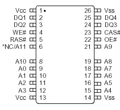
Features: • Industry-standard x4 pinout, timing, functions and packages• State-of-the-art, high-performance, low-power CMOS silicon-gate process• Single power supply (+3.3V ±0.3V or +5V ±10%)• All inputs, outputs and clocks are TTL-compatible• Refresh modes: RAS#-ONLY...
MT4LC4M4E8: Features: • Industry-standard x4 pinout, timing, functions and packages• State-of-the-art, high-performance, low-power CMOS silicon-gate process• Single power supply (+3.3V ±0.3V o...
SeekIC Buyer Protection PLUS - newly updated for 2013!
268 Transactions
All payment methods are secure and covered by SeekIC Buyer Protection PLUS.
Features: • Single +3.3V ±0.3V power supply• Industry-standard x4 pinout, timing, func...
Features: Single +3.3V ±0.3V power supplyIndustry-standard x4 pinout, timing, functions,and packag...
The 4 Meg x 4 DRAM MT4LC4M4E8 is a randomly accessed, solid-state memory containing 16,777,216 bits organized in a x4 configuration. RAS# is used to latch the row address (first 11 bits for 2K and first 12 bits for 4K). Once the page has been opened by RAS#, CAS# is used to latch the column address (the latter 11 bits for 2K and the latter 10 bits for 4K, address pins A10 and A11 are "don't care"). READ and WRITE cycles of MT4LC4M4E8 are selected with the WE# input.
A logic HIGH on WE# of MT4LC4M4E8 dictates READ mode, while a logic LOW on WE# dictates WRITE mode. During a WRITE cycle, data-in (D) is latched by the falling edge of WE# or CAS#, whichever occurs last. An EARLY WRITE occurs when WE# is taken LOW prior to CAS# falling. A LATE WRITE or READ-MODIFY-WRITE occurs when WE# falls after CAS# is taken LOW. During EARLY WRITE cycles, the data outputs (Q) of MT4LC4M4E8 will remain High-Z regardless of the state of OE#. During LATE WRITE or READ-MODIFYWRITE cycles, OE# must be taken HIGH to disable the data outputs prior to applying input data. If a LATE WRITE or READ-MODIFY-WRITE is attempted while keeping OE# LOW, no write will occur, and the data outputs of MT4LC4M4E8 will drive read data from the accessed location.
The four data inputs and the four data outputs of MT4LC4M4E8 are routed through four pins using common I/O, and pin direction is controlled by WE# and OE#.