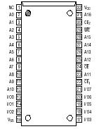
Features: • 131,072-wordx 8-bit configuration• Single 5 V power supply• Fully static operation• Operating temperature range: Ta = 0°C to 70°C• Power dissipation - Standby: 1 mA (Max.) - Operation: - 17 180 mA (Max.) - 20 170 mA (Max.) - 25 160 mA (Max.)• Access ...
MSM521008: Features: • 131,072-wordx 8-bit configuration• Single 5 V power supply• Fully static operation• Operating temperature range: Ta = 0°C to 70°C• Power dissipation - Stand...
SeekIC Buyer Protection PLUS - newly updated for 2013!
268 Transactions
All payment methods are secure and covered by SeekIC Buyer Protection PLUS.
Features: · 1,048,576-word × 1-bit configuration· Single 5 V power supply, ±10% tolerance· Input :...
Features: • 1,048,576-word ´ 16-bit configuration• Single 5 V power supply, ±10%...
• 131,072-word x 8-bit configuration
• Single 5 V power supply
• Fully static operation
• Operating temperature range: Ta = 0°C to 70°C
• Power dissipation
- Standby: 1 mA (Max.)
- Operation:
- 17 180 mA (Max.)
- 20 170 mA (Max.)
- 25 160 mA (Max.)
• Access time:
- 17 17 ns (Max.)
- 20 20 ns (Max.)
- 25 25 ns (Max.)
• (Input/Output) TTL compatible
• Power-down function by chip enable signal
• 3-state output
• Package:
- 32-pin 400 mil plastic SOJ (SOJ32-P-400-1.27) (Product : MSM521008-xxJS) xx indicates speed rank.
Parameter | Symbol | Condition | Rating | Unit |
Power Supply Voltage | VCC | Ta = 25°C, for VSS | 0.3 to 7.0 | V |
Pin Voltage | VT | 0.3* to VCC + 0.3 | V | |
Power Dissipation | PD | Ta = 25°C | 1.0 | W |
Operating Temperature | Topr | - | 0 to 70 | °C |
Storage Temperature | Tstg | - | 55 to 125 | °C |
The MSM521008 is a 131,072-word by 8-bit CMOS fast static RAM featuring a single 5 V power supply operation and direct TTL input/output compatibility. Since the circuitry is completely static, external clock and refreshing operations are unnecessary, making this device very easy to use. The MSM521008 uses NMOS cells and CMOS peripherals and provides high-speed operation at 17 ns access time. In addition, the MSM521008 is provided with a chip enable signal (CE1) suited to the expansion of a memory capacity, a chip enable signal (CE2) suited to the power-down function, and an output enable signal (OE) suited to the I/O bus line control.