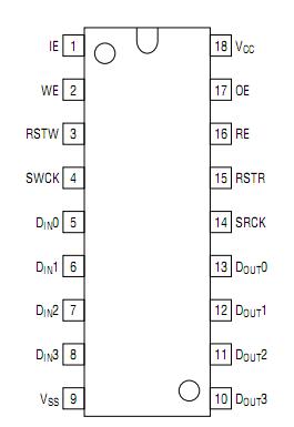
Features: · Single power supply: 5 V ±10%
· 512 Rows × 512 Column × 4 bits
· Fast FIFO (First-in First-out) operation
· High speed asynchronous serial access
Read/Write cycle time 30 ns/40 ns/60 ns
Access time 25 ns/30 ns/50 ns
· Direct cascading capability
· Write mask function (Input enable control)
· Data skipping function (Output enable control)
· Self refresh (No refresh control is required)
· Package:
18-pin 300 mil plastic DIP (DIP18-P-300-2.54-W1) (Product : MSM514223B-xxRS)
xx indicates speed rank.
Pinout Specifications
|
Parameter |
Symbol |
Condition |
Rating |
Unit |
| Input Output Voltage |
VT |
at Ta = 25, VSS |
1.0 to 7.0 |
V |
| Output Current |
IOS |
Ta = 25 |
50 |
mA |
| Power Dissipation |
PD |
Ta = 25 |
1 |
W |
| Operating Temperature |
Topr |
- |
0 to 70 |
|
| Storage Temperature |
Tstg |
- |
55 to 150 |
|
DescriptionThe OKI MSM514223B is a high performance 1-Mbit, 256K * 4-bit, Field Memory. It is designed for high-speed serial access applications such as HDTVs, conventional NTSC TVs, VTRs, digital movies and Multi-media systems. It is a FRAM for wide or low end use as general commodity TVs and VTRs, exclusively. The MSM514223B is not designed for the other use or high end use in medical systems, professional graphics systems which require long term picture, and data storage systems and others. The 1-Mbit capacity fits one field of a conventional NTSC TV screen and cascaded two MSM514223Bs make one frame of the screen: more than two MSM514223Bs can be cascaded directly without any delay devices among the MSM514223Bs. (Cascading of MSM514223B provides larger storage depth or a longer delay).
Each of the 4-bit planes has separate serial write and read ports that employ independent control clocks to support asynchronous read and write operations. Different clock rates are also supported that allow alternate data rates between write and read data streams.
The MSM514223B provides high speed FIFO, First-In First-Out, operation without external refreshing: it refreshes its DRAM storage cells automatically, so that it appears fully static to the users.
Moreover, fully static type memory cells and decoders for serial access enable refresh free serial access operation, so that serial read and/or write control clock can be halted high or low for any duration as long as the power is on. Internal conflicts of memory access and refreshing operations are prevented by special arbitration logic.
The MSM514223B's function is simple, and similar to a digital delay device whose delay-bit-length is easily set by reset timing. The delay length, number of read delay clocks between write and read, is determined by externally controlled write and read reset timings.
Additional SRAM serial registers, or line buffers for the initial access of 256 * 4-bit enable high speed first-bit-access with no clock delay just after the write or read reset timings.
The MSM514223B is similar in operation and functionality to OKI 1-Mbit Field Memory MSM514221B besides direct cascade capability. (As for MSM514221B operation compatible 2-Mbit Field Memory, OKI has MSM518221 as a sister device of MSM518222).
Additionally, the MSM514223B has write mask function or input enable function (IE), and read-data skipping function or output enable function (OE). The differences between write enable (WE) and input enable (IE), and between read enable (RE) and output enable (OE) are that WE and RE can stop serial write/read address increments but IE and OE can not stop the increment when write/read clocking is continuously applied to MSM514223B. The input enable (IE) function allows the user to write into selected locations of the memory only, leaving the rest of the memory contents unchanged. This facilitate data processing to display a "picture in picture" on a TV screen.

 MSM514223B Data Sheet


