MSC7119

Features: • StarCore® SC1400 DSP extended core with one SC1400 DSPcore, 256 Kbyte of internal SRAM M1 memory, 16 way 16 Kbyteinstruction cache (ICache), four-entry write buffer, programmableinterrupt controller (PIC), and low-power Wait and Stopprocessing modes.• 192 Kbyte M2 memor...

product image

MSC7119 Picture
SeekIC No. : 004427973 Detail

MSC7119: Features: • StarCore® SC1400 DSP extended core with one SC1400 DSPcore, 256 Kbyte of internal SRAM M1 memory, 16 way 16 Kbyteinstruction cache (ICache), four-entry write buffer, programmab...

floor Price/Ceiling Price

Part Number:
MSC7119
Supply Ability:
5000

Price Break

  • Qty
  • 1~5000
  • Unit Price
  • Negotiable
  • Processing time
  • 15 Days
Total Cost: $ 0.00

SeekIC Buyer Protection PLUS - newly updated for 2013!

  • Escrow Protection.
  • Guaranteed refunds.
  • Secure payments.
  • Learn more >>

Month Sales

268 Transactions

Rating

evaluate  (4.8 stars)

Upload time: 2024/11/26

Payment Methods

All payment methods are secure and covered by SeekIC Buyer Protection PLUS.

Notice: When you place an order, your payment is made to SeekIC and not to your seller. SeekIC only pays the seller after confirming you have received your order. We will also never share your payment details with your seller.
Product Details

Description


Features:

• StarCore® SC1400 DSP extended core with one SC1400 DSP
core, 256 Kbyte of internal SRAM M1 memory, 16 way 16 Kbyte
instruction cache (ICache), four-entry write buffer, programmable
interrupt controller (PIC), and low-power Wait and Stop
processing modes.
• 192 Kbyte M2 memory for critical data and temporary data buffering.
• 8 Kbyte boot ROM.
• AHB-Lite crossbar switch that allows parallel data transfers
between four master ports and six slave ports, where each port
connects to an AHB-Lite bus; fixed or round robin priority
programmable at each slave port; programmable bus parking at
each slave port; low power mode.
• Internal PLL generates up to 300 MHz clock for the SC1400 core
and up to 150 MHz for the crossbar switch, DMA channels, M2
memory, and other peripherals.
• Clock synthesis module provides predivision of PLL input clock;
independent clocking of the internal timers and DDR module;
programmable operation in the SC1400 low power Stop mode;
independent shutdown of different regions of the device.
• Enhanced 16-bit wide host interface (HDI16) provides a glueless
connection to industry-standard microcomputers,
microprocessors, and DSPs and can also operate with an 8-bit host
data bus, making if fully compatible with the DSP56300 HI08
from the external host side.
• DDR memory controller that supports byte enables for up to a
32-bit data bus; glueless interface to 150 MHz 14-bit page mode
DDR-RAM; 14-bit external address bus supporting up to 1 Gbyte;
and 16-bit or 32-bit external data bus.
• Programmable memory interface with independent read buffers,
programmable predictive read feature for each buffer, and a write buffer.
• System control unit performs software watchdog timer function;
includes programmable bus time-out monitors on AHB-Lite slave
buses; includes bus error detection and programmable time-out
monitors on AHB-Lite master buses; and has address
out-of-range detection on each crossbar switch buses.
• Event port collects and counts important signal events including
DMA and interrupt requests and trigger events such as interrupts,
breakpoints, DMA transfers, or wake-up events; units operate
independently, in sequence, or triggered externally; can be used
standalone or with the OCE10.
• Multi-channel DMA controller with 32 time-multiplexed
unidirectional channels, priority-based time-multiplexing
between channels using 32 internal priority levels, fixed- or
round-robin-priority operation, major-minor loop structure, and
DONE or DRACK protocol from requesting units.
• Two independent TDM modules with independent receive and
transmit, programmable sharing of frame sync and clock,
programmable word size (8 or 16-bit), hardware-base
A-law/-law conversion, up to 50 Mbps data rate per TDM, up to
128 channels, with glueless interface to E1/T1 frames and MVIP,
SCAS, and H.110 buses.
• Ethernet controller with support for 10/100 Mbps MII/RMII
designed to comply with IEEE Std. 802.3™, 802.3u™, 802.3x™,
and 802.3ac™; with internal receive and transmit FIFOs and a
FIFO controller; direct access to internal memories via its own
DMA controller; full and half duplex operation; programmable
maximum frame length; virtual local area network (VLAN) tag
and priority support; retransmission of transmit FIFO following
collision; CRC generation and verification for inbound and
outbound packets; and address recognition including
promiscuous, broadcast, individual address. hash/exact match,
and multicast hash match.
• UART with full-duplex operation up to 5.0 Mbps.
• Up to 41 general-purpose input/output (GPIO) ports.
• I2C interface that allows booting from EEPROM devices up to 1 Mbyte.
• Two quad timer modules, each with sixteen configurable 16-bit timers.
• fieldBIST™ unit detects and provides visibility into unlikely field
failures for systems with high availability to ensure structural
integrity, that the device operates at the rated speed, is free from
reliability defects, and reports diagnostics for partial or complete
device inoperability.
• Standard JTAG interface allows easy integration to system
firmware and internal on-chip emulation (OCE10) module.
• Optional booting external host via 8-bit or 16-bit access through
the HDI16, I2C, or SPI using in the boot ROM to access serial SPI
Flash/EEPROM devices; different clocking options during boot
with the PLL on or off using a variety of input frequency ranges.


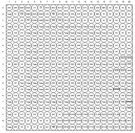
Pinout

  Connection Diagram


Specifications

Rating Symbol Value Unit
Core supply voltage VDDC 1.5 V
Memory supply voltage VDDM 4.0 V
PLL supply voltag VDDPLL 1.5 V
I/O supply voltage VDDIO 0.2 to 4.0 V
Input voltage VIN (GND 0.2) to 4.0 V
Reference voltage VREF 4.0 V
Maximum operating temperature TJ 105 °C
Minimum operating temperature TA -40 °C
Storage temperature range TSTG 55 to +150 °C
Notes: 1. Functional operating conditions are given in Table 3.
2. Absolute maximum ratings are stress ratings only, and functional operation at the maximum is not guaranteed. Stress beyond
the listed limits may affect device reliability or cause permanent damage.
3. Section 3.1, Thermal Design Considerations includes a formula for computing the chip junction temperature (TJ).


Customers Who Bought This Item Also Bought

Margin,quality,low-cost products with low minimum orders. Secure your online payments with SeekIC Buyer Protection.
LED Products
RF and RFID
Potentiometers, Variable Resistors
Sensors, Transducers
Computers, Office - Components, Accessories
View more