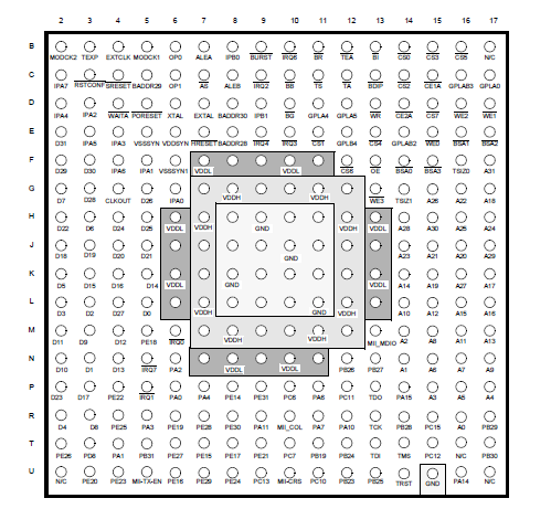
Features: The MPC875/870 is comprised of three modules that each use the 32-bit internal bus: a MPC8xx core, a system integration unit (SIU), and a communications processor module (CPM).
The following list summarizes the key MPC875/870 features:
• Embedded MPC8xx core up to 133 MHz
• Maximum frequency operation of the external bus is 80 MHz (in 1:1 mode)
- The 133-MHz core frequency supports 2:1 mode only.
- The 66-/80-MHz core frequencies support both the 1:1 and 2:1 modes.
• Single-issue, 32-bit core (compatible with the PowerPC architecture definition) with thirty-two 32-bit general-purpose registers (GPRs)
- The core performs branch prediction with conditional prefetch and without conditional execution.
- 8-Kbyte data cache and 8-Kbyte instruction cache (see Table 1)
Instruction cache is two-way, set-associative with 256 sets in 2 blocks
Data cache is two-way, set-associative with 256 sets
Cache coherency for both instruction and data caches is maintained on 128-bit (4-word) cache blocks.
Caches are physically addressed, implement a least recently used (LRU) replacement algorithm, and are lockable on a cache block basis.
- MMUs with 32-entry TLB, fully associative instruction and data TLBs
- MMUs support multiple page sizes of 4, 16, and 512 Kbytes, and 8 Mbytes; 16 virtual address spaces and 16 protection groups
- Advanced on-chip emulation debug mode
• Up to 32-bit data bus (dynamic bus sizing for 8, 16, and 32 bits)
• 32 address lines
• Memory controller (eight banks)
- Contains complete dynamic RAM (DRAM) controller
- Each bank can be a chip select or RAS to support a DRAM bank.
- Up to 30 wait states programmable per memory bank
- Glueless interface to DRAM, SIMMS, SRAM, EPROMs, Flash EPROMs, and other memory devices
- DRAM controller programmable to support most size and speed memory interfaces
- Four CAS lines, four WE lines, and one OE line
- Boot chip-select available at reset (options for 8-, 16-, or 32-bit memory)
- Variable block sizes (32 Kbyte256 Mbyte)
- Selectable write protection
- On-chip bus arbitration logic
• General-purpose timers
- Four 16-bit timers or two 32-bit timers
- Gate mode can enable/disable counting.
- Interrupt can be masked on reference match and event capture
• Two fast Ethernet controllers (FEC)-Two 10/100 Mbps Ethernet/IEEE 802.3 CDMA/CS that interface through MII and/or RMII interfaces
• System integration unit (SIU)
- Bus monitor
- Software watchdog
- Periodic interrupt timer (PIT)
- Clock synthesizer
- Decrementer and time base
- Reset controller
- IEEE 1149.1 test access port (JTAG)
• Security engine is optimized to handle all the algorithms associated with IPsec, SSL/TLS, SRTP, 802.11i, and iSCSI processing. Available on the MPC875, the security engine contains a crypto-channel, a controller, and a set of crypto hardware accelerators (CHAs). The CHAs are:
- Data encryption standard execution unit (DEU)
DES, 3DES
Two key (K1, K2, K1) or three key (K1, K2, K3)
ECB and CBC modes for both DES and 3DES
- Advanced encryption standard unit (AESU)
Implements the Rinjdael symmetric key cipher
ECB, CBC, and counter modes
128-, 192-, and 256-bit key lengths
- Message digest execution unit (MDEU)
SHA with 160- or 256-bit message digest
MD5 with 128-bit message digest
HMAC with either algorithm
- Master/slave logic, with DMA
32-bit address/32-bit data
Operation at 8xx bus frequency
- Crypto-channel supporting multi-command descriptors
Integrated controller managing crypto-execution units
Buffer size of 256 bytes for each execution unit, with flow control for large data sizes
• Interrupts
- Six external interrupt request (IRQ) lines
- 12 port pins with interrupt capability
- 23 internal interrupt sources
- Programmable priority between SCCs
- Programmable highest priority request
• Communications processor module (CPM)
- RISC controller
- Communication-specific commands (for example, GRACEFUL STOP TRANSMIT, ENTER HUNT MODE, and RESTART TRANSMIT)
- Supports continuous mode transmission and reception on all serial channels
- 8-Kbytes of dual-port RAM
- Several serial DMA (SDMA) channels to support the CPM
- Three parallel I/O registers with open-drain capability
• On-chip 16 * 16 multiply accumulate controller (MAC)
- One operation per clock (two-clock latency, one-clock blockage)
- MAC operates concurrently with other instructions
- FIR loop-Four clocks per four multiplies
• Four baud-rate generators
- Independent (can be connected to any SCC or SMC)
- Allows changes during operation
- Autobaud support option
• SCC (serial communication controller)
- Ethernet/IEEE 802.3 optional on the SCC, supporting full 10-Mbps operation
- HDLC/SDLC
- HDLC bus (implements an HDLC-based local area network (LAN))
- Asynchronous HDLC to support point-to-point protocol (PPP)
- AppleTalk
- Universal asynchronous receiver transmitter (UART)
- Synchronous UART
- Serial infrared (IrDA)
- Binary synchronous communication (BISYNC)
- Totally transparent (bit streams)
- Totally transparent (frame based with optional cyclic redundancy check (CRC))
• SMC (serial management channel)
- UART (low-speed operation)
- Transparent
• Universal serial bus (USB)-Supports operation as a USB function endpoint, a USB host controller, or both for testing purposes (loopback diagnostics)
- USB 2.0 full-/low-speed compatible
- The USB function mode has the following features:
Four independent endpoints support control, bulk, interrupt, and isochronous data transfers.
CRC16 generation and checking
CRC5 checking
NRZI encoding/decoding with bit stuffing
12- or 1.5-Mbps data rate
Flexible data buffers with multiple buffers per frame
Automatic retransmission upon transmit error
- The USB host controller has the following features:
Supports control, bulk, interrupt, and isochronous data transfers
CRC16 generation and checking
NRZI encoding/decoding with bit stuffing
Supports both 12- and 1.5-Mbps data rates (automatic generation of preamble token and data rate configuration). Note that low-speed operation requires an external hub.
Flexible data buffers with multiple buffers per frame
Supports local loopback mode for diagnostics (12 Mbps only)
• Serial peripheral interface (SPI)
- Supports master and slave modes
- Supports multiple-master operation on the same bus
• Inter-integrated circuit (I2C) port
- Supports master and slave modes
- Supports a multiple-master environment
• The MPC875 has a time-slot assigner (TSA) that supports one TDM bus (TDMb).
- Allows SCC and SMC to run in multiplexed and/or non-multiplexed operation
- Supports T1, CEPT, PCM highway, ISDN basic rate, ISDN primary rate, user defined
- 1- or 8-bit resolution
- Allows independent transmit and receive routing, frame synchronization, and clocking
- Allows dynamic changes
- Can be internally connected to two serial channels (one SCC and one SMC)
• PCMCIA interface
- Master (socket) interface, release 2.1-compliant
- Supports one independent PCMCIA socket on the MPC875/MPC870
- 8 memory or I/O windows supported
• Debug interface
- Eight comparators: four operate on instruction address, two operate on data address, and two operate on data
- Supports conditions: = < >
- Each watchpoint can generate a break point internally.
• Normal high and normal low power modes to conserve power
• 1.8-V core and 3.3-V I/O operation with 5-V TTL compatibility
• The MPC875/870 comes in a 256-pin ball grid array (PBGA) package.
Pinout Specifications
|
Rating |
Symbol |
Value |
Unit |
| Supply voltage 1 |
VDDL (corevoltage) |
0.3 to 3.4 |
V |
|
VDDH (I/Ovoltage) |
0.3 to 3.4 |
V |
|
VDDSYN |
0.3 to 3.4 |
V |
|
Differencebetween
VDDL andVDDSYN |
<100 |
mV |
| Input voltage 2 |
Vin |
GND 0.3 to
VDDH |
V |
| Storage temperature range |
Tstg |
55 to +150 |
|
1 The power supply of the device must start its ramp from 0.0 V.
2 Functional operating conditions are provided with the DC electrical specifications in Table 6. Absolute maximum ratings are stress ratings only; functional operation at the maxima is not guaranteed. Stress beyond those listed may
affect device reliability or cause permanent damage to the device. Caution: All inputs that tolerate 5 V cannot be more than 2.5 V greater than VDDH. This restriction applies t o power up and normal operation (that is, if the MPC875/870 is unpowered, a voltage greater than 2.5 V must not be applied to its inputs).
DescriptionThe MPC875/MPC870 is a versatile single-chip integrated microprocessor and peripheral combination that can be used in a variety of controller applications and communications and networking systems. The MPC875/MPC870 provides enhanced ATM functionality over that of other ATM-enabled members of the MPC860 family.

 MPC875 Data Sheet


