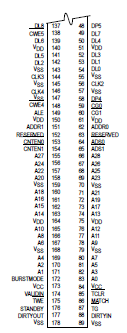
Features: • PowerPCstyle Burst Counter on Chip• FlowThrough Data I/O• Plug and Pin Compatibility• Multiple Clock Pins for Reduced Loading• All Cache Data and Tag I/Os are LVTTL (3.3 V) Compatible• Three State Outputs• Byte Write Capability• Fast Modu...
MPC2106C: Features: • PowerPCstyle Burst Counter on Chip• FlowThrough Data I/O• Plug and Pin Compatibility• Multiple Clock Pins for Reduced Loading• All Cache Data and Tag I/Os a...
SeekIC Buyer Protection PLUS - newly updated for 2013!
268 Transactions
All payment methods are secure and covered by SeekIC Buyer Protection PLUS.
Rating |
Symbol |
Value |
Unit |
Power Supply Voltage |
VCC |
0.5 to + 7.0 |
V |
Voltage Relative to VSS |
Vin, Vout |
0.5 to VCC + 0.5 |
V |
Output Current (per I/O) Data RAM Tag |
Iout |
± 30 ± 20 |
mA |
Power Dissipation MPC2105C MPC2106C |
PD |
4.6 9.2 |
W |
Temperature Under Bias |
Tbias |
10 to + 85 |
|
Operating Temperature |
TA |
0 to +70 |
|
Storage Temperature |
Tstg |
55 to + 125 |
|
NOTE:
Permanent device damage may occur if ABSOLUTE MAXIMUM RATINGS are exceeded. Functional operation should be restricted to RECOMMENDED OPERATING CONDITIONS. Exposure to higher than recommended voltages for extended periods of time could affect device reliability.
This device contains circuitry to protect the inputs against damage due to high static voltages or electric fields; however, it is advised that normal precautions be taken to avoid application of any voltage higher than maximum rated voltages to this highimpedance circuit.
This BiCMOS memory circuit has been designed to meet the dc and ac specifications shown in the tables, after thermal equilibrium has been established.
This device contains circuitry that will ensure the output devices are in HighZ at power up.
The MPC2105C and the MPC2106C are designed to provide burstable, high performance L2 cache for the PowerPC 60x microprocessor family in conformance with the PowerPC Reference Platform (PReP) and the PowerPC Common Hardware Reference Platform (CHRP) specifications.
The MPC2105C and MPC2106C utilize synchronous BurstRAMs. The modules are configured as 64K x 72, and 128K x 72 bits in a 178 (89 x 2) pin DIMM format. The MPC2105C uses four of the 3 V 64K x 18; the MPC2106C uses eight of the 3 V 64K x 18. For tag bits, a 5 V cache tag RAM configured as 16K x 12 for tag field plus 16K x 2 for valid and dirty status bits is used.
Bursts can be initiated with the ADS signal. Subsequent burst addresses are generated internal to the BurstRAM by the CNTEN signal.
Write cycles of MPC2105C and MPC2106C are internally self timed and are initiated by the rising edge of the clock (CLKx) inputs. Eight write enables are provided for byte write control.
Write cycles are internally self timed and are initiated by the rising edge of the clock CLKx) inputs. Eight write enables are provided for byte write control.
Presence detect pins are available for auto configuration of the cache control.
The MPC2105C and MPC2106C family pinout will support 5 V and 3.3 V components for a clear path to lower voltage and power savings. Both power supplies must be connected.
All of these cache modules are plug and pin compatible with each other.