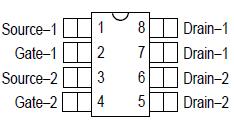
Features: New Features of TMOS V• Onresistance Area Product about Onehalf that of Standard MOSFETs with New Low Voltage, Low RDS(on) Technology• Faster Switching than EFET PredecessorsFeatures Common to TMOS V and TMOS EFETS• Avalanche Energy Specified• IDSS and VDS(on) Spe...
MMDF2N06VL: Features: New Features of TMOS V• Onresistance Area Product about Onehalf that of Standard MOSFETs with New Low Voltage, Low RDS(on) Technology• Faster Switching than EFET PredecessorsFe...
SeekIC Buyer Protection PLUS - newly updated for 2013!
268 Transactions
All payment methods are secure and covered by SeekIC Buyer Protection PLUS.
New Features of TMOS V
• Onresistance Area Product about Onehalf that of Standard MOSFETs with New Low Voltage, Low RDS(on) Technology
• Faster Switching than EFET Predecessors
Features Common to TMOS V and TMOS EFETS
• Avalanche Energy Specified
• IDSS and VDS(on) Specified at Elevated Temperature
• Static Parameters are the Same for both TMOS V and TMOS EFET
• Miniature SO8 Surface Mount Package Saves Board Space
• Mounting Information for SO8 Package Provided
Rating |
Symbol |
Value |
Unit |
DraintoSource Voltage |
VDSS |
25 |
Vdc |
GatetoSource Voltage - Continuous |
VGS |
± 20 |
Vdc |
Drain Current - Continuous @ TA = 25 Drain Current - Continuous @ TA = 100 Drain Current - Single Pulse (tp 10 ms) |
ID |
2.5 |
Adc |
Total Power Dissipation @ TA = 25 (2) Derate above 25 |
PD |
2.0 |
W |
Operating and Storage Temperature Range |
TJ, Tstg |
55 to 150 |
|
Single Pulse DraintoSource Avalanche Energy - Starting TJ = 25 (VDD = 20 Vdc, VGS = 10 Vdc, Peak IL = 7.0 Apk, L = 10 mH, RG = 25 ) |
EAS |
245 |
mJ |
Thermal Resistance, Junction to Ambient (2) |
RJA |
62.5 |
/W |
Maximum Lead Temperature for Soldering Purposes, 0.0625, from case for 10 seconds |
TL |
260 |
TMOS V is a new MMDF2N06VL technology designed to achieve an onresistance area product about onehalf that of standard MOSFETs. This new technology more than doubles the present cell density of our 50 and 60 volt TMOS devices. Just as with our TMOS EFET designs, TMOS V is designed to withstand high energy in the avalanche and commutation modes. Designed for low voltage, high speed switching applications in power supplies, converters and power motor controls, these MMDF2N06VLs are particularly well suited for bridge circuits where diode speed and commutating safe operating areas are critical and offer additional safety margin against unexpected voltage transients.