Features: • Single 3.3 V ± 5% Power Supply
• Fast Access Times: 6/8/10 ns Max
• Sustained Throughput of 1.49 Gigabits/Second
• Single Clock Operation
• Address, Data Input, E1, E2, PT, W, and Data Output Registers on Chip
• 83 MHz Maximum Clock Cycle Time
• Self Timed Write
• Separate Data Input and Data Output Pins
• PassThrough Feature
• Asynchronous Output Enable (G)
• LVTTL Compatible I/O
• No Dead Cycles Required for Reads after Writes or for Writes after Reads
• 100 Pin TQFP Package
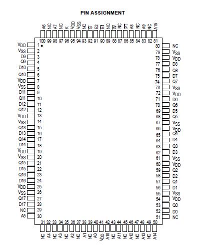
• Simultaneous Reads and WritesPinout
Specifications
| Rating |
Symbo |
Value |
Unit |
| Power Supply Voltage |
VDD |
0.5 to + 4.6 |
V |
Voltage Relative to VSS for Any Pin
Except VDD |
Vin, Vout |
0.5 to VDD + 0.5 |
V |
| Output Current |
Iout |
± 20 |
mA |
| Power Dissipation |
PD |
TBD |
W |
| Temperature Under Bias |
Tbias |
10 to + 85 |
°C |
| Operating Temperature |
TA |
0 to + 70 |
°C |
| Storage Temperature - Plastic |
Tstg |
55 to + 125 |
°C |
NOTE: Permanent device damage may occur if ABSOLUTE MAXIMUM RATINGS are exceeded. Functional operation should be restricted to RECOMMENDED OPERATING CONDITIONS. Exposure to higher than recommended voltages for extended periods of time could affect device reliability.
DescriptionThe Motorola MCM69Q618 is a 1 Megabit static random access memory, organized as 64K words of 18 bits. It features separate data input and data output buffers and incorporates input and output registers on board with high speed SRAM.
The MCM69Q618 allows the user to perform transparent write and data pass through. Two data bus ports are provided a data input (D) and a data output (Q) port. The synchronous design allows for precise cycle control with the use of an external single clock (K). Address port, data input (D0 D17), data output (Q0 Q17), write enable (W), chip enables (E1, E2), and passthrough enable (PT) are registered on the rising edge of clock (K).
Any given cycle operates on only one address. However, for any cycle, reads and writes can be intermixed. Thus, one can perform a read, a write, or a combination read/ write during any one cycle. For a combination read/write, the contents of the array are read before the new data is written.
By using the passthrough function, the output port Q can be made to reflect either the contents of the array or the data presented to the input port D. For read/write or a read cycle with G low, the Q port will output the contents of the array. However, if PT is asserted, the Q port will instead output the data presented at the D input port.

 MCM69Q618 Data Sheet


