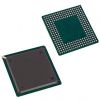
Features: • Single 3.3 V ±5% Power Supply• Fast Access Times: 6/8/10 ns Max• Sustained Throughput of 2.98 Gigabits/Second• Single Clock Operation• Address, Data Input,E1 , E2, PT , W , and Data Output Registers on Chip• 83 MHz Maximum Clock Cycle Time• Sel...
MCM69Q536: Features: • Single 3.3 V ±5% Power Supply• Fast Access Times: 6/8/10 ns Max• Sustained Throughput of 2.98 Gigabits/Second• Single Clock Operation• Address, Data Input,E...
SeekIC Buyer Protection PLUS - newly updated for 2013!
268 Transactions
All payment methods are secure and covered by SeekIC Buyer Protection PLUS.
Rating | Symbol | Value | Unit |
Power Supply Voltage | VDD | 0.5 to +4.6 | V |
Voltage Relative to VSSfor Any Pin Except VDD |
Vin, Vout | 0.5 to VDD+0.5 | V |
Output Current | Iout | ±20 | mA |
Power Dissipation | PD | TBD | W |
Temperature Under Bias | Tbias | 10 to + 85 | °C |
Operating Temperature | TA | 0 to + 70 | °C |
Storage Temperature - Plastic | Tstg | 55 to + 125 | °C |
The Motorola MCM69Q536 is a 1 Megabit static random access memory, organized as 32K words of 36 bits. It features separate data input and data output buffers and incorporates input and output registers on board with high speed SRAM.
The MCM69Q536 allows the user to perform transparent writes and data pass through. Two data bus ports are provided - a data input (D) and a data output (Q) port.
The synchronous design of the MCM69Q536 allows for precise cycle control with the use of an external single clock (K). Address port, data input (D0 D35), data output (Q0 Q35), write en-able (w ), chip enables (E1 , E2), and passthrough enable (PT ) are registered on the rising edge of clock (K). Any given cycle operates on only one address. However, for any cycle, reads and writes can be intermixed. Thus, one can perform a read, a write, or a combination read/write during any one cycle. For a combination read/write, the contents of the array are read before the new data is written.
By using the passthrough function of the MCM69Q536, the output port Q can be made to reflect either the contents of the array or the data presented to the input port D. For read/write or a read cycle with G low, the Q port will output the contents of the array. However, if PT is asserted, the Q port will instead output the data presented at the D input port.