Features: • MCM69P8183.5: 3.5 ns Access/6 ns Cycle (166 MHz)
MCM69P8183.8: 3.8 ns Access/6.7 ns Cycle (150 MHz)
MCM69P8184: 4 ns Access/7.5 ns Cycle (133 MHz)
• 3.3 V + 10%, 5% Core Power Supply, 2.5 V or 3.3 V I/O Supply
• ADSP, ADSC, andADV Burst Control Pins
• Selectable Burst Sequencing Order (Linear/Interleaved)
• 2Cycle Deselect Timing
• Internally SelfTimed Write Cycle
• Byte Write and Global Write Control
• PB1 Version 2.0 Compatible
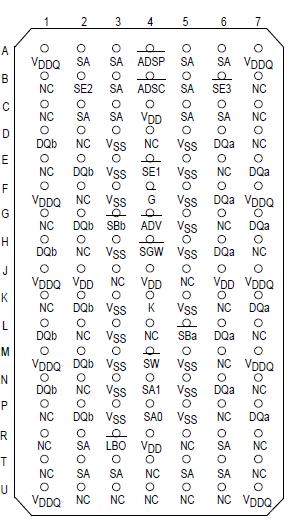
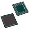
• JEDEC Standard 119Pin PBGA PackagePinout Specifications
|
Rating |
Symbol |
Value |
Unit |
Notes |
| Power Supply Voltage |
VDD |
VSS 0.5 to + 4.6 |
V |
|
| I/O Supply Voltage |
VDDQ |
VSS 0.5 to VDD |
V |
2 |
Input Voltage Relative to VSS for Any
Pin Except VDD |
Vin, Vout |
VSS 0.5 to
VDD + 0.5 |
V |
2 |
| Input Voltage (ThreeState I/O) |
VIT |
VSS 0.5 to
VDDQ + 0.5 |
V |
2 |
| Output Current (per I/O) |
Iout |
± 20 |
mA |
|
| Package Power Dissipation |
PD |
1.6 |
W |
3 |
| Ambient Temperature |
TA |
0 to 70 |
°C |
|
| Die Temperature |
TJ |
110 |
°C |
3 |
| Temperature Under Bias |
Tbias |
10 to 85 |
°C |
|
| Storage Temperature |
Tstg |
55 to 125 |
°C |
|
DescriptionThe MCM69P818 is a 4Mbit synchronous fast static RAM designed to provide a burstable, high performance, secondary cache for the PowerPC and other high performance microprocessors. It is organized as 256K words of 18 bits each.
The features of MCM69P818 can be summarized as:(1)MCM69P8183.5: 3.5 ns Access/6 ns Cycle (166 MHz); (2)MCM69P8183.8: 3.8 ns Access/6.7 ns Cycle (150 MHz); (3)MCM69P8184: 4 ns Access/7.5 ns Cycle (133 MHz); (4)3.3 V + 10%, 5% Core Power Supply, 2.5 V or 3.3 V I/O Supply; (5)ADSP, ADSC, and ADV Burst Control Pins; (6)Selectable Burst Sequencing Order (Linear/Interleaved); (7)2Cycle Deselect Timing; (8)Internally SelfTimed Write Cycle; (9)Byte Write and Global Write Control; (10)PB1 Version 2.0 Compatible; (11)JEDEC Standard 119Pin PBGA Package.
The absolute maximum ratings of MCM69P818 are:(1)Power Supply Voltage:VSS0.5V to + 4.6V; (2)I/O Supply Voltage:VSS0.5V to VDD ; (3)Input Voltage Relative to VSS for Any Pin Except VDD:VSS-0.5V to VDD+0.5V; (4)Input Voltage (ThreeState I/O):VSS-0.5V to VDDQ+0.5V; (5)Output Current (per I/O):±20 mA; (6)Package Power Dissipation:1.6 W; (7)Ambient Temperature:0°C to 70 °C; (8)Die Temperature:110 °C; (9)Temperature Under Bias Tbias: -10°C to 85 °C; (10)Storage Temperature Tstg:-55°C to 125 °C.
If you want to know more information such as the electrical characteristics about the MCM69P818, please download the datasheet in www.seekic.com or www.chinaicmart.com .

 MCM69P818 Data Sheet


