Features: • MCM69P7364: 4 ns Access/7.5 ns Cycle (133 MHz)• 3.3 V + 10%, 5% Core Power Supply, 2.5 V or 3.3 V I/O Supply• ADSP, ADSC, and ADV Burst Control Pins• Selectable Burst Sequencing Order (Linear/Interleaved)• TwoCycle Deselect Timing• Internally SelfTi...
MCM69P736: Features: • MCM69P7364: 4 ns Access/7.5 ns Cycle (133 MHz)• 3.3 V + 10%, 5% Core Power Supply, 2.5 V or 3.3 V I/O Supply• ADSP, ADSC, and ADV Burst Control Pins• Selectable ...
SeekIC Buyer Protection PLUS - newly updated for 2013!
268 Transactions
All payment methods are secure and covered by SeekIC Buyer Protection PLUS.
Rating | Symbol | Value | Unit | Notes |
Power Supply Voltage | VDD | VSS 0.5 to + 4.6 | V | |
I/O Supply Voltage | VDDQ | VSS 0.5 to VDD | V | 2 |
Input Voltage Relative to VSS for Any Pin Except VDD |
Vin, Vout | VSS 0.5 to VDD + 0.5 |
V | 2 |
Input Voltage (ThreeState I/O) | VIT | VSS 0.5 to VDDQ + 0.5 |
V | 2 |
Output Current (per I/O) | Iout | ± 20 | mA | |
Package Power Dissipation | PD | 1.6 | W | 3 |
Ambient Temperature | TA | 0 to 70 | °C | |
Die Temperature | TJ | 110 | °C | 3 |
Temperature Under Bias | Tbias | 10 to 85 | °C | |
Storage Temperature | Tstg | 55 to 125 | °C |
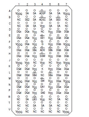
The MCM69P736 is a 4M bit synchronous fast static RAM designed to provide a burstable, high performance, secondary cache for the PowerPCE and other high performance microprocessors. It is organized as 128K words of 36 bits each. This device integrates input registers, an output register, a 2bit address counter, and high speed SRAM onto a single monolithic circuit for reduced parts count in cache data RAM applications. Synchronous design allows precise cycle control with the use of an external clock (K).
Addresses (SA), data inputs (DQx) of the MCM69P736, and all control signals except output enable (G) and linear burst order (LBO) are clock (K) controlled through positive edgetriggered noninverting registers.
Bursts can be initiated with either ADSP or ADSC input pins. Subsequent burst addresses can be generated internally by the MCM69P736 (burst sequence operates in linear or interleaved mode dependent upon the state of LBO) and controlled by the burst address advance (ADV) input pin.
Write cycles of the MCM69P736 are internally selftimed and are initiated by the rising edge of the clock (K) input. This feature eliminates complex offchip write pulse generation and provides increased timing flexibility for incoming signals.
Synchronous byte write (SBx), synchronous global write (SGW), and synchronous write enable (SW) are provided to allow writes to either individual bytes or to all bytes. The four bytes are designated as "a", "b", "c", and "d". SBa controls DQa, SBb controls DQb, etc. Individual bytes are written if the selected byte writes SBx are asserted with SW. All bytes are written if either SGW is asserted or if all SBx and SW are asserted.
For read cycles, pipelined SRAMs output data of the MCM69P736 is temporarily stored by an edgetriggered output register and then released to the output buffers at the next rising edge of clock (K).
The MCM69P736 operates from a 3.3 V core power supply and all outputs operate on a 2.5 V or 3.3 V power supply. All inputs and outputs are JEDEC standard JESD85 compatible.