Specifications Rating Symbol Value Unit Power Supply Voltage VDD VSS 0.5 to + 4.6 V I/O Supply Voltage (See Note 2) VDDQ VSS 0.5 to VDD V Input Voltage Relative to VSS for AnyPin Except VDD (See Note 2) Vin, Vout VSS 0.5 toVDD + 0.5 V Input Voltage (ThreeState I/O)(...
MCM69F735: Specifications Rating Symbol Value Unit Power Supply Voltage VDD VSS 0.5 to + 4.6 V I/O Supply Voltage (See Note 2) VDDQ VSS 0.5 to VDD V Input Voltage Relative to VSS for A...
SeekIC Buyer Protection PLUS - newly updated for 2013!
268 Transactions
All payment methods are secure and covered by SeekIC Buyer Protection PLUS.
Rating | Symbol | Value | Unit |
Power Supply Voltage | VDD | VSS 0.5 to + 4.6 | V |
I/O Supply Voltage (See Note 2) | VDDQ | VSS 0.5 to VDD | V |
Input Voltage Relative to VSS for Any Pin Except VDD (See Note 2) |
Vin, Vout | VSS 0.5 to VDD + 0.5 |
V |
Input Voltage (ThreeState I/O) (See Note 2) |
VIT | VSS 0.5 to VDDQ + 0.5 |
V |
Output Current (per I/O) | Iout | ± 20 | mA |
Package Power Dissipation (See Note 3) | PD | 1.6 | W |
Temperature Under Bias | Tbias | 10 to 85 | |
Storage Temperature | Tstg | 55 to 125 |
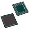
The MCM69F735 is a 4M bit synchronous fast static RAM designed to provide a burstable, high performance, secondary cache for the PowerPCE and other high performance microprocessors. It is organized as 128K words of 36 bits each. This device integrates input registers, a 2bit address counter, and high speed SRAM onto a single monolithic circuit for reduced parts count in cache data RAM applications. Synchronous design allows precise cycle control with the use of an external clock (K).
Addresses (SA), data inputs (DQx), and all control signals except outputenable (G) and linear burst order (LBO) are clock (K) controlled through positiveedgetriggered noninverting registers.
Bursts can be initiated with either ADSP or ADSC input pins. Subsequent burst addresses can be generated internally by the MCM69F735 (burst sequence operates in linear or interleaved mode dependent upon the state of LBO) and controlled by the burst address advance (ADV) input pin.
Write cycles are internally selftimed and are initiated by the rising edge of the clock (K) input. This feature eliminates complex offchip write pulse generation and provides increased timing flexibility for incoming signals.
Synchronous byte write (SBx), synchronous global write (SGW), and synchronous write enable (SW) are provided to allow writes to either individual bytes or to all bytes. The four bytes are designated as "a", "b", "c", and "d". SBa controls DQa, SBb controls DQb, etc. Individual bytes are written if the selected byte writes SBx are asserted with SW. All bytes are written if either SGW is asserted or if all SBx and SW are asserted.
For read cycles, a flowthrough SRAM allows output data to simply flow freely from the memory array.
The MCM69F735 operates from a 3.3 V core power supply and all outputs operate on a 3.3 V or 2.5 V power supply. All inputs and outputs are JEDEC standard JESD85 compatible.