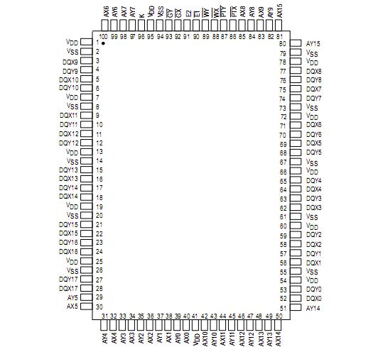
Pinout Specifications
|
Rating |
Symbol |
Value |
Unit |
|
Power Supply Voltage |
VDD |
0.5 to + 4.6 |
V |
Voltage Relative to VSS for Any Pin
Except VDD |
Vin, Vout |
0.5 to VDD + 0.5 |
V |
|
Output Current |
Iout |
± 20 |
mA |
|
Power Dissipation |
PD |
TBD |
W |
|
Temperature Under Bias |
Tbias |
10 to + 85 |
|
| Operating Temperature |
TA |
0 to + 70 |
|
|
Storage Temperature - Plastic |
Tstg |
55 to + 125 |
|
Description
The MCM69D618 is a 1Mbit static random access memory, organized as 64Kwords of 18 bits. It features commondata input and data output buffers andincorporates input and output registers onboard with high speedSRAM.
The MCM69D618 allows the user to concurrently perform reads, writes, orpassthrough cycles in combination onthe two data ports. The two address ports(AX, AY) determine the read or write locations for theirrespective data ports(DQX, DQY).
The synchronous design allows for precise cycle control with the use of anexternal single clock (K). All signal pins except output enables (GX,GY) areregistered on the rising edge of clock (K).
The passthrough feature allows data to be passed from one port to the other,in either direction. The PTXinput must be asserted to pass data from port X toport Y. The PTX will likewise pass data from port Y toport X. A passthroughoperation takes precedence over a read operation.PTY the case when AX and AY are thesame, certain protocols are followed. Ifboth ports are read, the reads occur normally. If one port iswritten and the otheris read, the read from the array will occur before the data is written. If both portsare written, only the data on DQY will be written to the array.
• Single 3.3 V ± 5% Power Supply
• Fast Access Times: 6/8 ns Max
• Throughput of 1.49 Gigabits/Second
• Single Clock Operation
• Address, Data Input, E1, E2, PTX, PTY, WX, WY, and Data Output RegistersOnChip
• 83 MHz Maximum Clock Frequency
• Self Timed Write
• Two BiDirectional Data Buses
• Can be Configured as Separate I/O
• PassThrough Feature
• Asynchronous Output Enables (GX, GY)
• LVTTL Compatible I/O
• Concurrent Reads and Writes
• 100Pin TQFP Package

 MCM69D618 Data Sheet


