Features: • Single 5 V ± 5% Power Supply• Fast Access Times: 9/11/14 ns Max and Cycle Times: 12.5/15/20 ns Min• Byte Writeable via Dual Write Strobes• Internal Input Registers (Address, Data, Control)• Internally SelfTimed Write Cycle• TSP, TSC, andBAA Burst Con...
MCM67M518: Features: • Single 5 V ± 5% Power Supply• Fast Access Times: 9/11/14 ns Max and Cycle Times: 12.5/15/20 ns Min• Byte Writeable via Dual Write Strobes• Internal Input Register...
SeekIC Buyer Protection PLUS - newly updated for 2013!
268 Transactions
All payment methods are secure and covered by SeekIC Buyer Protection PLUS.
Rating | Symbol | Value | Unit |
Power Supply Voltage | VCC | 0.5 to + 7.0 | V |
Voltage Relative to VSS for Any Pin Except VCC |
Vin, Vout | 0.5 to VCC + 0.5 | V |
Output Current (per I/O) | Iout | ± 30 | mA |
Power Dissipation | PD | 1.6 | W |
Temperature Under Bias | Tbias | 10 to + 85 | |
Operating Temperature | TA | 0 to +70 | |
Storage Temperature | Tstg | 55 to + 125 |
The MCM67M518 is a 589,824 bit synchronous static random access memory designed to provide a burstable, highperformance, secondary cache for the MC68040 and PowerPCE microprocessors. It is organized as 32,768 words of 18 bits, fabricated using Motorola's highperformance silicongate BiCMOS technology. The device integrates input registers, a 2bit counter, high speed SRAM, and high drive capability outputs onto a single monolithic circuit for reduced parts count implementation of cache data RAM applications. Synchronous design allows precise cycle control with the use of an external clock (K).
BiCMOS circuitry reduces the overall power consumption of the integrated functions for greater reliability.
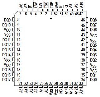
Addresses (A0 A14), data inputs (DQ0 DQ17), and all control signals, except output enable (G), are clock (K) controlled through positiveedgetriggered noninverting registers.
Bursts can be initiated with either transfer start processor (TSP) or transfer start cache controller (TSC) input pins. Subsequent burst addresses are generated internally by the MCM67M518 (burst sequence imitates that of the MC68040 and PowerPC) and controlled by the burst address advance (BAA) input pin. The following pages provide more detailed information on burst controls.
Write cycles are internally selftimed and are initiated by the rising edge of the clock (K) input. This feature eliminates complex offchip write pulse generation and provides increased flexibility for incoming signals.
Dual write enables (LW and UW) are provided to allow individually writeable bytes. LW controls DQ0 DQ8 (the lower bits), while UW controls DQ9 DQ17 (the upper bits).
This MCM67M518 is ideally suited for systems that require wide data bus widths and cache memory.