Features: •Single 5 V ± 5% Power Supply
•Fast Access Times: 10/12/15 ns Max
•Byte Writeable via Dual Write Enables
•Separate Data Input Latch for Simplified Write Cycles
•Address and Chip Enable Input Latches
•Common Data Inputs and Data Outputs
•Output Enable Controlled ThreeState Outputs
•3.3 V I/O Compatible
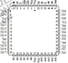
•High Board Density 52Lead PLCC PackagePinout Specifications
| Rating |
Symbol |
Value |
Unit |
| Power Supply Voltage |
VCC |
0.5 to 7.0 |
V |
Voltage Relative to VSS for Any
Pin Except VCC |
Vin,Vout |
0.5 to VCC + 0.5 |
V |
| Output Current (per I/O) |
Iout |
±30 |
mA |
| Power Dissipation |
PD |
1.6 |
W |
| Temperature Under Bias |
Tbias |
10 to + 85 |
°C |
| Operating Temperature |
TA |
0 to + 70 |
°C |
| Storage Temperature |
Tstg |
55 to + 125 |
°C |
DescriptionThe MCM67A618 is a 1,179,648 bit latched address static random access memory organized as 65,536 words of 18 bits, fabricated with Motorola's high
performance silicongate BiCMOS technology. The device integrates a 64K x 18SRAM core with advanced peripheral circuitry consisting of address and data in
-put latches, active low chip enable, separate upper and lower byte write strobes,and a fast output enable. This device has increased output drive capability sup-ported by multiple power pins.
Address,data in, and chip enable latches are provided. When latch enables(AL for address and chip enables and DL for data in) are high, the address, data in, and chip enable latches are in the transparent state. If latch enables are tied high the device can be used as an asynchronous SRAM. When latch enables are low the address, data in, and chip enable latches are in the latched state. This input latch simplifies read and write cycles by guaranteeing address and datain hold time in a simple fashion.
Dual write enables (LW</a> and UW</a>) are provided to allow individually writeable bytes. LW</a> controls DQ0 DQ8 (the lower bits) while UW</a> controls DQ9 DQ17 (the upper bits).
Six pair of power and ground pins have been utilized and placed on the pack-age for maximum performance.
The MCM67A618 will be available in a 52pin plastic leaded chip carrier(PLCC).
This device is ideally suited for systems that require wide data bus widths, cache memory, and tag RAMs.

 MCM67A618 Data Sheet


