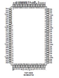
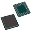
Features: • 3.3 V LVTTL and LVCMOS Compatible• MCM63Z736/MCM63Z818133 = 4.2 ns Access/7.5 ns Cycle (133 MHz) MCM63Z736/MCM63Z818100 = 5 ns Access/10 ns Cycle (100 MHz) • Selectable Burst Sequencing Order (Linear/Interleaved)• Internally SelfTimed Write Cycle• TwoCycle...
MCM63Z736: Features: • 3.3 V LVTTL and LVCMOS Compatible• MCM63Z736/MCM63Z818133 = 4.2 ns Access/7.5 ns Cycle (133 MHz) MCM63Z736/MCM63Z818100 = 5 ns Access/10 ns Cycle (100 MHz) • Selectable...
SeekIC Buyer Protection PLUS - newly updated for 2013!
268 Transactions
All payment methods are secure and covered by SeekIC Buyer Protection PLUS.
Rating | Symbol | Value | Unit | Notes |
Power Supply Voltage | VDD | 0.5 to + 4.6 | V | |
I/O Supply Voltage | VDDQ | VSS 0.5 to VDD | V | 2 |
Input Voltage Relative to VSS for Any Pin Except VDD |
Vin, Vout | 0.5 to VDD + 0.5 | V | 2 |
Input Voltage (Three State I/O) | VIT | VSS 0.5 to VDDQ + 0.5 |
V | 2 |
Output Current (per I/O) | Iout | ± 20 | mA | |
Package Power Dissipation | PD | 1.3 | W | 3 |
Temperature Under Bias | Tbias | 10 to 85 | ||
Storage Temperature | Tstg | 55 to 125 |
The ZBT RAM is a 4Mbit synchronous fast static RAM designed to provide zero bus turnaround. The ZBT RAM allows 100% use of bus cycles during backtoback read/write and write/read cycles. The MCM63Z736 is organized as 128K words of 36 bits each and the MCM63Z818 is organized as 256K words of 18 bits each, fabricated with high performance silicon gate CMOS technology. This device integrates input registers, an output register, a 2bit address counter, and high speed SRAM onto a single monolithic circuit for reduced parts count in communication applications. Synchronous design allows precise cycle control with the use of an external clock (CK). CMOS circuitry reduces the overall power consumption of the integrated functions for greater reliability.
Addresses (SA), data inputs (DQ), and all control signals except output enable (G) and linear burst order (LBO) are clock (CK) controlled through positive edgetriggered noninverting registers.
Write cycles of the MCM63Z736 are internally selftimed and are initiated by the rising edge of the clock (CK) input. This feature eliminates complex offchip write pulse generation and provides increased timing flexibility for incoming signals.
For read cycles, pipelined SRAM output data of the MCM63Z736 is temporarily stored by an edge triggered output register and then released to the output buffers at the next rising edge of clock (CK).