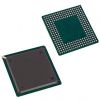
MCM63R818

Specifications Symbol Parameter Value Unit VDD Core Supply Voltage 0.5 to 3.9 V VDDQ Output Supply Voltage 0.5 to 2.5 V Vin Voltage On Any Pin Other Than JTAG 0.5 to 2.5 V VJTAG Voltage On Any JTAG Pin 0.5 to 3.9 V Iin Input Cur...

product image

MCM63R818 Picture
SeekIC No. : 004417833 Detail

MCM63R818: Specifications Symbol Parameter Value Unit VDD Core Supply Voltage 0.5 to 3.9 V VDDQ Output Supply Voltage 0.5 to 2.5 V Vin Voltage On Any Pin Other Tha...

floor Price/Ceiling Price

Part Number:
MCM63R818
Supply Ability:
5000

Price Break

  • Qty
  • 1~5000
  • Unit Price
  • Negotiable
  • Processing time
  • 15 Days
Total Cost: $ 0.00

SeekIC Buyer Protection PLUS - newly updated for 2013!

  • Escrow Protection.
  • Guaranteed refunds.
  • Secure payments.
  • Learn more >>

Month Sales

268 Transactions

Rating

evaluate  (4.8 stars)

Upload time: 2024/11/27

Payment Methods

All payment methods are secure and covered by SeekIC Buyer Protection PLUS.

Notice: When you place an order, your payment is made to SeekIC and not to your seller. SeekIC only pays the seller after confirming you have received your order. We will also never share your payment details with your seller.
Product Details

Description


Specifications

Symbol
Parameter
Value
Unit
VDD
Core Supply Voltage
0.5 to 3.9
V
VDDQ
Output Supply Voltage
0.5 to 2.5
V
Vin
Voltage On Any Pin Other Than JTAG
0.5 to 2.5
V
VJTAG
Voltage On Any JTAG Pin
0.5 to 3.9
V
Iin
Input Current (per I/O)
±50
mA
Iout
Output Current (per I/O)
± 25
mA
TA
Operating Temperature
0 to 70
W
Tbias
Temperature Under Bias
10 to 85
°C
Tstg
Storage Temperature
55 to 125
°C

NOTE: Permanent device damage may occur if ABSOLUTE MAXIMUM RATINGS are exceeded. Functional operation should be restricted to RECOMMENDED OPERATING CONDITIONS. Exposure to higher than recommended voltages for
extended periods of time could affect device reliability.


Description

The MCM63R736/818 is a 4Mbit synchronous late write fast static RAM designed to provide high performance in secondary cache and ATM switch,Telecom, and other high speed memory applications. The MCM63R818 (organized as 256K words by 18 bits), and the MCM63R736 (organized as 128K words by 36 bits) are fabricated in Motorola's high performance silicon gate copper CMOS technology.

The differential clock (CK) inputs control the timing of read/write operations of the RAM. At the rising edge of CK, all addresses, write enables, and synchronous selects are registered. An internal buffer and special logic enable the memory to accept write data on the rising edge of CK, a cycle after address and control signals.Read data is also driven on the rising edge of CK.

The RAM uses HSTL inputs and outputs. The adjustable input trippoint (Vref) and output voltage (VDDQ) gives the system designer greater flexibility in optimizing system performance.The synchronous write and byte enables allow writing to individual bytes or the entire word.

The impedance of the output buffers is programmable, allowing the outputs to match the impedance of the circuit traces which reduces signal reflections.
• Byte Write Control
• 2.5 V 5% to 3.3 V +10% Operation
• 2.375 V to 3.6 V Operation
• HSTL - I/O (JEDEC Standard JESD86 Class I Compatible)
• HSTL - User Selectable Input TripPoint
• HSTL - Compatible Programmable Impedance Output Drivers
• Register to Register Synchronous Operation
• Boundary Scan (JTAG) IEEE 1149.1 Compatible
• Differential Clock Inputs
• Optional x18 or x36 Organization
• MCM63R736/8183 = 3 ns
   MCM63R736/8183.3 = 3.3 ns
   MCM63R736/8183.7 = 3.7 ns
   MCM63R736/8184 = 4 ns
• Sleep Mode Operation (ZZ pin)
• 119Bump, 50 mil (1.27 mm) Pitch, 14mm x 22mm Flipped Chip Plastic Ball Grid Array (PBGA) Package


Customers Who Bought This Item Also Bought

Margin,quality,low-cost products with low minimum orders. Secure your online payments with SeekIC Buyer Protection.
Soldering, Desoldering, Rework Products
Resistors
Sensors, Transducers
Integrated Circuits (ICs)
Transformers
View more