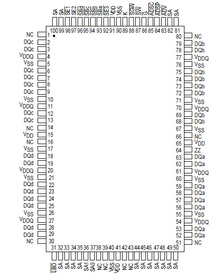
Pinout Specifications
|
Rating |
Symbol |
Value |
Unit |
Notes |
| Power Supply Voltage |
VDD |
0.5 to 4.6 |
V |
|
| I/O Supply Voltage |
VDDQ |
VSS0.5 to VDD |
V |
2 |
Input Voltage Relative to VSS for
Any Pin Except VDD |
Vin.Vout |
0.5 to VDD + 0.5 |
V |
2 |
| Input Voltage (Three State I/O) |
VIT |
VSS0.5 to
VDDQ + 0.5 |
V |
2 |
| Output Current (per I/O) |
Iout |
±20 |
mA |
|
| Package Power Dissipation |
PD |
1.3 |
W |
3 |
| Temperature Under Bias |
Tbias |
10 to 85 |
|
|
| Storage Temperature |
Tstg |
55 to 125 |
|
|
NOTES:
1. Permanent device damage may occur if ABSOLUTE MAXIMUM RATINGS are exceeded. Functional operation should be restricted to RECOMMENDED OPERATING CONDITIONS. Exposure to higher than recommended voltages for extended periods of time could affect device reliability.
2. This is a steadystate DC parameter that is in effect after the power supply has achieved its nominal operating level. Power sequencing is not necessary.
3. Power dissipation capability is dependent upon package characteristics and use environment. See Package Thermal Characteristics.
DescriptionThe MCM63F733A and SCM63F733A are 4Mbit synchronous fast static RAMs designed to provide a burstable, high performance, secondary cache for the PowerPCE and other high performance microprocessors. They are organized as 128K words of 32 bits each, fabricated with high performance silicon gate CMOS technology. This device integrates input registers, a 2bit address counter, and high speed SRAM onto a single monolithic circuit for reduced parts count in cache data RAM applications. Synchronous design allows precise cycle control with the use of an external clock (K). CMOS circuitry reduces the overall power consumption of the integrated functions for greater reliability.
Addresses (SA), data inputs (DQx), and all control signals except output enable (G) and Linear Burst Order (LBO) are clock (K) controlled through positiveedgetriggered noninverting registers.
Bursts can be initiated with either ADSP or ADSC input pins. Subsequent burst addresses can be generated internally by the MCM63F733A and SCM63F733A (burst sequence operates in linear or interleaved mode dependent upon state of LBO) and controlled by the burst address advance (ADV) input pin.
Write cycles are internally selftimed and are initiated by the rising edge of the clock (K) input. This feature eliminates complex offchip write pulse generation and provides increased timing flexibility for incoming signals.
Synchronous byte write (SBx), synchronous global write (SGW), and synchronous write enable (SW) are provided to allow writes to either individual bytes or to all bytes. The four bytes are designated as "a", "b", "c", and "d". SBa controls DQa, SBb controls DQb, etc. Individual bytes are written if the selected byte writes SBx are asserted with SW. All bytes are written if either SGW is asserted or if all SBx and SW are asserted.
For read cycles, a flowthrough SRAM allows output data to simply flow freely from the memory array.
The MCM63F733A and SCM63F733A operate from a 3.3 V core power supply and all outputs operate on a 2.5 V or 3.3 V power supply. All inputs and outputs are JEDEC Standard JESD85 compatible.
• MCM63F733A8.5 = 8.5 ns Access
MCM63F733A9 = 9 ns Access
MCM63F733A/SCM63F733A10 = 10 ns Access
MCM63F733A/SCM63F733A11 = 11 ns Access
• 3.3 V + 10%/ 5% Core, Power Supply, 2.5 V or 3.3 V I/O Supply
• ADSP, ADSC, and ADV Burst Control Pins
• Selectable Burst Sequencing Order (Linear/Interleaved)
• Internally SelfTimed Write Cycle
• Byte Write and Global Write Control
• SingleCycle Deselect
• Sleep Mode (ZZ)
• 40 to 85°C Extended Operating Temperatures (SCM63F733A only)
• 100Pin TQFP Package

 MCM63F733A Data Sheet


