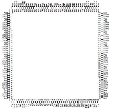
Application- ATM - Ethernet Switches - Routers - Cellular Base Stations- Cell/Frame Buffers - SNA Switches - Shared Memory - RAID SystemsPinoutSpecifications Symbol Parameter Value Unit VDD Power Supply Voltage 0.5 to 4.6 V Vin,Vout Voltage Relative to VSS for An...
MCM63D736A: Application- ATM - Ethernet Switches - Routers - Cellular Base Stations- Cell/Frame Buffers - SNA Switches - Shared Memory - RAID SystemsPinoutSpecifications Symbol Parameter Value U...
SeekIC Buyer Protection PLUS - newly updated for 2013!
268 Transactions
All payment methods are secure and covered by SeekIC Buyer Protection PLUS.
Symbol |
Parameter |
Value |
Unit |
VDD |
Power Supply Voltage |
0.5 to 4.6 |
V |
Vin,Vout |
Voltage Relative to VSS for Any Pin Except VDD |
0.5 to VDD + 0.5 |
V |
Iout |
Output Current per |
± 20 |
mA |
PD |
Package Power Dissipation |
1.6 |
W |
Tbias |
Temperature Under Bias |
10 to 85 |
°C |
Tstg |
Storage Temperature- Plastic |
55 to 150 |
°C |
NOTES:
1. Permanent device damage may occur if ABSOLUTE MAXIMUM RATINGS are exceeded. Functional operation should be restricted to RECOMMENDED OPERATING CONDITIONS. Exposure to higher than recommended voltages for extended periods of time could affect device reliability.
2. Power dissipation capability is dependent upon package characteristics and use environment. See Package Thermal Characteristics.
The MCM63D736A is a 4Mbit static random access memory, organized as 128K words of 36 bits. It features common data input and data output buffers and incorporates input and output registers onboard with high speed SRAM.
The MCM63D736A allows the user to concurrently perform reads, writes, or passthrough cycles in combination on the two data ports. The two address ports (AX, AY) determine the read or write locations for their respective data ports (DQX, DQY).
The synchronous design allows for precise cycle control with the use of an external single clock (K). All signal pins except output enables (GX, GY) are registered on the rising edge of clock (K).
The passthrough feature allows data to be passed from one port to the other,in either direction. The PTX input must be asserted to pass data from port X to port Y. The PTY will likewise pass data from port Y to port X. A passthrough
operation takes precedence over a read operation.
For the case when AX and AY are the same, certain protocols are followed. If both ports are read, the reads occur normally. If one port is written and the other is read, the read from the array will occur before the data is written. If both ports are written, only the data on DQY will be written to the array.
• Single 3.3 V ±5% Power Supply
• 133 MHz Maximum Clock Frequency
• Throughput of 4.8 Gigabits/Second
• Single Clock Operation
• SelfTimed Write
• Two BiDirectional Data Buses
• Can be Configured as Separate I/O
• PassThrough Feature
• Asynchronous Output Enables (GX, GY)
• LVTTL Compatible I/O
• Concurrent Reads and Writes
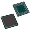
• 176Pin TQFP Package