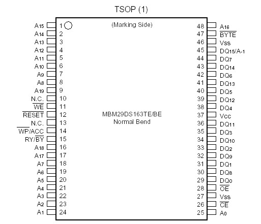
MBM29DS163TE/BE10

Features: • 0.23 mm Process Technology• Simultaneous Read/Write Operations (Dual Bank)-Host system can program or erase in one bank, and then read immediately and simultaneously from the-bank with zero latency between read and write operations-Read-while-erase-Read-while-program•...

product image

MBM29DS163TE/BE10 Picture
SeekIC No. : 004414093 Detail

MBM29DS163TE/BE10: Features: • 0.23 mm Process Technology• Simultaneous Read/Write Operations (Dual Bank)-Host system can program or erase in one bank, and then read immediately and simultaneously from the...

floor Price/Ceiling Price

Part Number:
MBM29DS163TE/BE10
Supply Ability:
5000

Price Break

  • Qty
  • 1~5000
  • Unit Price
  • Negotiable
  • Processing time
  • 15 Days
Total Cost: $ 0.00

SeekIC Buyer Protection PLUS - newly updated for 2013!

  • Escrow Protection.
  • Guaranteed refunds.
  • Secure payments.
  • Learn more >>

Month Sales

268 Transactions

Rating

evaluate  (4.8 stars)

Upload time: 2024/11/27

Payment Methods

All payment methods are secure and covered by SeekIC Buyer Protection PLUS.

Notice: When you place an order, your payment is made to SeekIC and not to your seller. SeekIC only pays the seller after confirming you have received your order. We will also never share your payment details with your seller.
Product Details

Description


Features:

• 0.23 mm Process Technology
• Simultaneous Read/Write Operations (Dual Bank)
-Host system can program or erase in one bank, and then read immediately and simultaneously from the
-bank with zero latency between read and write operations
-Read-while-erase
-Read-while-program
• Single 1.8 V Read, Program, and Erase Minimized system level power requirements
• Compatible with JEDEC-standard Commands Use the same software commands as E2PROMs
• Compatible with JEDEC-standard Worldwide Pinouts
-48-pin TSOP (1) (Package suffix : TN - Normal Bend Type, TR - Reversed Bend Type)
-48-ball FBGA (Package suffix : PBT)
• Minimum 100,000 Program/Erase Cycles
• High Performance 100 ns maximum access time
• Sector Erase Architecture
-Eight 4 K word and thirty-one 32 K word sectors in word mode
-Eight 8 K byte and thirty-one 64 K byte sectors in byte mode
-Any combination of sectors can be concurrently erased. Also supports full chip erase.
• Boot Code Sector Architecture
-T = Top sector
-B = Bottom sector
• HiddenROM Region
-64 K byte of HiddenROM, accessible through a new "HiddenROM Enable" command sequence
-Factory serialized and protected to provide a secure electronic serial number (ESN)
• WP/ACC Input Pin
-At VIL, allows protection of boot sectors, regardless of sector protection/unprotection status
-At VIH, allows removal of boot sector protection
-At VACC, increases program performance
• Embedded EraseTM* Algorithms Automatically pre-programs and erases the chip or any sector
• Embedded ProgramTM* Algorithms Automatically writes and verifies data at specified address
• Data Polling and Toggle Bit feature for detection of program or erase cycle completion
• Ready/Busy output (RY/BY)
Hardware method for detection of program or erase cycle completion
• Automatic Sleep Mode When addresses remain stable, automatically switch themselves to low power mode.
• Program Suspend/Resume
• Erase Suspend/Resume Suspends the erase operation to allow a read data and/or program in another sector within the same device
• Sector Group Protection Hardware method disables any combination of sector groups from program or erase operations
• Sector Group Protection Set function by Extended sector group protection command
• Fast Programming Function by Extended Command
• Temporary Sector Group Unprotection Temporary sector group unprotection via the RESET pin.


Pinout

  Connection Diagram


Specifications

Parameter
Conditions
Rating
Units
Min
Max
Storage Temperature
Tstg
55
+125
°C
Ambient Temperature with Power Applied
TA
40
+85
°C
Voltage with Respect to Ground All Pins except
A9, OE, RESET *1, *2
VIN, VOUT
0.5
VCC+0.5
V
Power Supply Voltage *1
VCC
0.5
+3.0
V
A9, OE, andRESET *1, *3
VIN
0.5
+11.5
V


Description

The MBM29DS163TE/BE10 is 16 M-bit, 1.8 V-only Flash memory organized as 2 M bytes of 8 bits each or 1 M words of 16 bits each. The device is offered in 48-pin TSOP (1) and 48-ball FBGA packages. This device is designed to be programmed in system with standard system 1.8 V VCC supply. 12.0 V VPP and 5.0 V VCC are not required for write or erase operations. MBM29DS163TE/BE10 can also be reprogrammed in standard EPROM programmers.


Customers Who Bought This Item Also Bought

Margin,quality,low-cost products with low minimum orders. Secure your online payments with SeekIC Buyer Protection.
Motors, Solenoids, Driver Boards/Modules
Boxes, Enclosures, Racks
Resistors
Soldering, Desoldering, Rework Products
Crystals and Oscillators
View more