MBM29DL640E

Features: • 0.23 mm Process Technology• Simultaneous Read/Write operations (Dual Bank)• FlexBankTM Bank A : 8 Mbit (8 KB* 8 and 64 KB * 15) Bank B : 24 Mbit (64 KB * 48) Bank C : 24 Mbit (64 KB * 48) Bank D : 8 Mbit (8 KB * 8 and 64 KB * 15) Two virtual Banks are chosen from the ...

product image

MBM29DL640E Picture
SeekIC No. : 004414088 Detail

MBM29DL640E: Features: • 0.23 mm Process Technology• Simultaneous Read/Write operations (Dual Bank)• FlexBankTM Bank A : 8 Mbit (8 KB* 8 and 64 KB * 15) Bank B : 24 Mbit (64 KB * 48) Bank C : 2...

floor Price/Ceiling Price

Part Number:
MBM29DL640E
Supply Ability:
5000

Price Break

  • Qty
  • 1~5000
  • Unit Price
  • Negotiable
  • Processing time
  • 15 Days
Total Cost: $ 0.00

SeekIC Buyer Protection PLUS - newly updated for 2013!

  • Escrow Protection.
  • Guaranteed refunds.
  • Secure payments.
  • Learn more >>

Month Sales

268 Transactions

Rating

evaluate  (4.8 stars)

Upload time: 2024/11/27

Payment Methods

All payment methods are secure and covered by SeekIC Buyer Protection PLUS.

Notice: When you place an order, your payment is made to SeekIC and not to your seller. SeekIC only pays the seller after confirming you have received your order. We will also never share your payment details with your seller.
Product Details

Description


Features:

• 0.23 mm Process Technology
• Simultaneous Read/Write operations (Dual Bank)
• FlexBankTM
   Bank A : 8 Mbit (8 KB * 8 and 64 KB * 15)
   Bank B : 24 Mbit (64 KB *  48)
   Bank C : 24 Mbit (64 KB * 48)
   Bank D : 8 Mbit (8 KB *  8 and 64 KB *  15)
   Two virtual Banks are chosen from the combination
   of four physical banks (Refer to Table 9, 10)
   Host system can program or erase in one bank, and then read
   immediately and simultaneously from the other
   bank with zero latency between read and write operations.
   Read-while-erase
   Read-while-program
• Single 3.0 V read, program, and erase
   Minimized system level power requirements
• Compatible with JEDEC-standard commands
   Uses the same software commands as E2PROMs
• Compatible with JEDEC-standard world-wide pinouts
   48-pin TSOP (I) (Package suffix : TN - Normal Bend Type, TR - Reversed Bend Type)
   63-ball FBGA (Package suffix : PBT)
• Minimum 100,000 program/erase cycles
• High performance 80 ns maximum access time
• Sector erase architecture
   Sixteen 4 Kword and one hundred twenty-six 32 Kword sectors in word mode
   Sixteen 8 Kbyte and one hundred twenty-six 64 Kbyte sectors in byte mode
   Any combination of sectors can be concurrently erased. It also supports full chip erase.
• Hidden ROM (Hi-ROM) region
   256 byte of Hi-ROM, accessible through a new "Hi-ROM Enable" command sequence
   Factory serialized and protected to provide a secure electronic serial number (ESN)
• WP/ACC input pin
   At VIL, allows protection of "outermost" 2* 8 Kbytes on both ends of boot
   sectors, regardless of sector protection/ unprotection status
   At VIH, allows removal of boot sector protection
   At VACC, increases program performance
• Embedded EraseTM Algorithms
   Automatically preprograms and erases the chip or any sector
• Embedded ProgramTM Algorithms
   Automatically writes and verifies data at specified address
• Data Polling and Toggle Bit feature for detection of program or erase cycle completion
• Ready/Busy output (RY/BY)
   Hardware method for detection of program or erase cycle completion
• Automatic sleep mode When addresses remain stable,
   the device automatically switches itself to low power mode.
• Low VCC write inhibit £ 2.5 V
• Program Suspend/Resume Suspends the program
   operation to allow a read in another byte
• Erase Suspend/Resume Suspends the erase operation to allow
   a read data and/or program in another sector within the same device
• Sector group protection Hardware method disables any combination
   of sector groups from program or erase operations
• Sector Group Protection Set function by Extended sector group protection command
• Fast Programming Function by Extended Command
• Temporary sector group unprotection
   Temporary sector group unprotection via the RESET pin.
• In accordance with CFI (Common Flash Memory Interface)


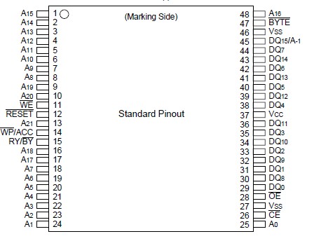
Pinout

  Connection Diagram


Specifications

Parameter

Symbol

Rating

Unit

Min.

Max.

Storage Temperature

Tstg

-55

+125

°C

Ambient Temperature with Power Applied

Ta

-40

+85

°C

Voltage with Respect to Ground All pins except A9, OE, and RESET (Note 1)

VIN,VOUT

-0.5

VCC + 0.5

V

Power Supply Voltage (Note 1)

VCC

-0.5

+4.0

V

A9, OE, and RESET (Note 2)

VIN

-0.5

+13.0

V

WP/ACC (Note 3)

VACC

-0.5

+10.5

V


Description

The MBM29DL640E is a 64 M-bit, 3.0 V-only Flash memory organized as 8 Mbytes of 8 bits each or 4 Mwords of 16 bits each. The device is offered in 48-pin TSOP (I) and 63-ball FBGA packages. This device is designed to be programmed in system with 3.0 V VCC supply. 12.0 V VPP and 5.0 V VCC are not required for write or erase operations. The device can also be reprogrammed in standard EPROM programmers.

MBM29DL640E is organized into four physical banks: Bank A, Bank B, Bank C and Bank D, which can be considered to be four separate memory arrays as far as certain operations are concerned. This device is the same as Fujitsu's standard 3 V only Flash memories with the additional capability of allowing a normal non-delayed read access from a non-busy bank of the array while an embedded write (either a program or an erase) operation is simultaneously taking place on the other bank.


Customers Who Bought This Item Also Bought

Margin,quality,low-cost products with low minimum orders. Secure your online payments with SeekIC Buyer Protection.
Integrated Circuits (ICs)
Power Supplies - Board Mount
Computers, Office - Components, Accessories
Circuit Protection
Memory Cards, Modules
Resistors
View more