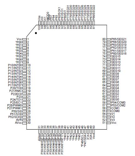
Features: • Package
QFP, LQFP package for MB89F499, MB89498 MQFP package for MB89PV490
• High speed operating capability at low voltage
• Minimum execution time : 0.32 ms/12.5 MHz
• F2MC-8L family CPU core
Instruction set optimized for controllers:
Multiplication and division instructions
16-bit arithmetic operations
Branch instructions by test bit
Bit manipulation instructions, etc.
• PLL circuit for sub-clock
· Embedded for PLL clock multiplication circuit for sub-clock
·Operating clock (PLL for sub-clock) can be selected from no multiplication or 4 times of the sub-clock oscillation frequency.
• 6 timers
PWM timer × 2
8/16-bit timer/counter × 2
21-bit timebase timer
Watch prescaler
• External interrupt
Edge detection (selectable edge) : 8 channels
Low level interrupt (wake-up function) : 8 channels
• 10-bit A/D converter (8 channels) 10-bit successive approximation type
• UART/SIO Synchronous/asynchronous data transfer capability
• SIO Switching of synchronous data transfer capability
• LCD controller/driver Max 32 segments output × 4 commons
• I2C interface circuit
• Remote receiver circuit
• Low-power consumption mode
Stop mode (oscillation stops so as to minimize the current consumption.)
Sleep mode (CPU stops so as to reduce the current consumption to approx. 1/3 of normal.)
Watch mode (operation except the watch prescaler stops so as to reduce the power comsumption to an
extremely low level.)
Sub-clock mode
• Watchdog timer reset
• I/O ports : Max 66 channels
Pinout Specifications
|
Parameter |
Symbol |
Min |
Max |
Unit |
Remarks |
| Power supply voltage*1 |
VCC |
VSS - 0.3 |
VSS + 4.0 |
V |
AVCC must be equal to VCC |
|
AVCC |
VSS - 0.3 |
VSS + 4.0 |
V |
|
AVR |
VSS - 0.3 |
VSS + 4.0 |
V |
|
| LCD power supply voltage |
V1 to V3 |
VSS - 0.3 |
VCC |
V |
|
| Input voltage*1 |
VI |
VSS - 0.3 |
VCC + 0.3 |
V |
Except P40 to P47 |
|
VSS - 0.3 |
VSS + 6.0 |
V |
P40 to P47 in MB89PV490 and MB89498 |
|
VSS - 0.3 |
VSS + 5.5 |
V |
|
| Output voltage*1 |
VO |
VSS - 0.3 |
VSS + 0.3 |
V |
|
| Maximum clamp current |
ICLAMP |
-2.0 |
+2.0 |
mA |
*2 |
Total maximum clamp
current |
|ICLAMP| |
- |
20 |
mA |
*2 |
"L" level maximum
output current |
IOL |
- |
15 |
mA |
|
"L" level average
current |
IOLAV |
- |
4 |
mA |
Average value (operating current* operating rate) |
| "L" level total maximum output current |
IOL |
- |
100 |
mA |
|
| "L" level total average output current |
IOLAV |
- |
50 |
mA |
Average value (operating current* operating rate) |
"H" level maximum
output current |
IOH |
- |
-15 |
mA |
|
"H" level average
current |
IOHAV |
- |
-4 |
mA |
Average value (operating current* operating rate) |
"H" level maximum
total output current |
IOH |
- |
-50 |
mA |
|
| "H" level average total output current |
IOHAV |
- |
-20 |
mA |
Average value (operating current* operating rate) |
| Power consumption |
PD |
- |
300 |
mW |
|
| Operating temperature |
TA |
-40 |
+85 |
°C |
|
*1 : The parameter is based on AVSS = VSS = 0.0 V.
*2 : ` Applicable to pins : P00 to P07, P10 to P17, P20 to P27, P30 to P37, P50 to P52, P80 to P82
` Use within recommended operating conditions.
` Use at DC voltage (current) .
` The +B signal should always be applied with a limiting resistance placed between the +B signal and the microcontroller.
` The value of the limiting resistance should be set so that when the +B signal is applied the input current to the microcontroller pin does not exceed rated values, either instantaneously or for prolonged periods.
` Note that when the microcontroller drive current is low, such as in the power saving modes, the +B input potential may pass through the protective diode and increase the potential at the VCC pin, and this may affect other devices.
` Note that if a +B signal is input when the microcontroller current is off (not fixed at 0 V) , the power supply is provided from the pins, so that incomplete operation may result.
` Note that if the +B input is applied during power-on, the power supply is provided from the pins and the resulting supply voltage may not be sufficient to operate the power-on result.
` Care must be taken not to leave the +B input pin open.
` Note that analog system input/output pins other than the A/D input pins (LCD drive pins, comparator input pins, etc.) cannot accept +B signal input.
DescriptionThe MB89498 series has been developed as a general-purpose version of the F2MC*-8L family consisting of proprietary 8-bit single-chip microcontrollers.
In addition to a compact instruction set, the general-purpose, single-chip microcontroller contains a variety of peripheral functions such as 21-bit timebase timer, watch prescaler, PWM timer, 8/16-bit timer/counter, remote receiver circuit, LCD controller/driver, external interrupt 0 (edge) , external interrupt 1 (level) , 10-bit A/D converter, UART/SIO, SIO, I2C and watchdog timer reset.
The MB89498 series is designed suitable for compact disc/radio receiver controller as well as in a wide range of applications for consumer product.

 MB89498 Data Sheet


