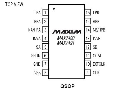
Features: Dual 2nd-Order Filter in a 16-Pin QSOP Package
High Accuracy
Q Accuracy: ±0.2%
Clock-to-Ce nter Frequency Error: ±0.2%
Rail-to-Rail Input and Output Operation
Single-Supply Operation: +5V (MAX7490) or +3V (MAX7491)
Internal or External Clock
Highpass, Lowpass, Bandpass, and Notch Filters
Clock-to-Center Frequency Ratio of 100:1
Internal Sampling-to-Center Frequency Ratio of 200:1
Center Frequency up to 40kHz
Easily Cascaded for Multipole Filters
Low-Power Shutdown: <1µA Supply CurrentApplicationTunable Active Filters
Multipole Filters
ADC Anti-Aliasing
Post-DAC Filtering
Adaptive Filtering
Phase-Locked Loops (PLLs)
Set-Top Boxes
Typical Application Circuit appears at end of data sheet.
Rail-to-Rail is a registered trademark of Nippon Motorola, Ltd.Pinout Specifications
VDD to GND..............................................................-0.3V to +6V
EXTCLK, SHDN to GND .............................................-0.3V to +6V
INV_, LP_, BP_, N_/HP_, S_, COM,
CLK to GND................................................-0.3V to (VDD + 0.3V)
Maximum Current into Any Pin ...........................................50mA
Continuous Power Dissipation (TA = +70°C)
16-Pin QSOP (derate 8.30mW/°C above +70°C).........667mW
Operating Temperature Range
MAX749_CEE ......................................................0°C to +70°C
MAX749_EEE....................................................-40°C to +85°C
Die Temperature ...........................................................+150°C
Storage Temperature.....................................-65°C to +150°C
Lead Temperature (soldering, 10s) ...............................+300°C
Stresses beyond those listed under "Absolute Maximum Ratings" may cause permanent damage to the device. These are stress ratings only, and functional operation of the device at these or any other conditions beyond those indicated in the operational sections of the specifications is not implied. Exposure to absolute maximum rating conditions for extended periods may affect device reliability.
DescriptionThe MAX7490/MAX7491 consist of two identical lowpower, low-voltage, wide dynamic range, Rail-to-Rail®, 2nd-order switched-capacitor building blocks. Each of the two filter sections, together with two to four external resistors, can generate all standard 2nd-order functions: bandpass, lowpass, highpass, and notch (band reject). Three of these functions are simultaneously available. Fourth-order filters can be obtained by cascading the two 2nd-order filter sections. Similarly, higher order filters can easily be created by cascading multiple MAX7490/MAX7491s.
Two clocking options of MAX7490 are available: self-clocking (through the use of an external capacitor) or external clocking for tighter cutoff frequency control. The lockto- center frequency ratio is 100:1. Sampling is done at twice the clock frequency, further separating the cutoff frequency and Nyquist frequency.
The MAX7490/MAX7491 have an internal rail splitter that establishes a precise common voltage needed for single-supply operation. The MAX7490 operates from a single +5V supply and the MAX7491 operates from a single +3V supply. Both devices feature a low-power shutdown mode and come in a 16-pin QSOP package.

 MAX7490 Data Sheet


