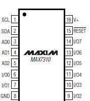
Features: ` 400kHz 2-Wire Interface` 2.3V to 5.5V Operation` Low Standby Current (1.7A typ)` Bus Timeout for Lock-Up-Free Operation` 56 Slave ID Addresses` Polarity Inversion` Eight I/O Pins that Default to Inputs on Power-Up` 5V Tolerant Open-Drain Output on I/O0` 4mm x 4mm, 0.8mm Thin QFN Packag...
MAX7310: Features: ` 400kHz 2-Wire Interface` 2.3V to 5.5V Operation` Low Standby Current (1.7A typ)` Bus Timeout for Lock-Up-Free Operation` 56 Slave ID Addresses` Polarity Inversion` Eight I/O Pins that De...
SeekIC Buyer Protection PLUS - newly updated for 2013!
268 Transactions
All payment methods are secure and covered by SeekIC Buyer Protection PLUS.
V+ to GND ..............................................................-0.3V to +6V
I/O1I/O7 as an Input....................(VSS - 0.3V) to (VDD + 0.3V)
I/O0 as an Input...........................................(VSS - 0.3V) to +6V
SCL, SDA, AD0, AD1, AD2, RESET ..................(VSS - 0.3V) to +6V
DC Current on I/O0 ....................................................... +400A
DC Current on I/O1 to I/O7 ........................................... ±50mA
Maximum GND and V+ Current.........................................180mA
Continuous Power Dissipation (TA = +70)
16-Pin TSSOP (derate 5.7mW/ above +70) ..............457mW
16-Pin QSOP (derate 8.3mW/ above +70)................667mW
16-Pin Thin QFN (derate 16.9mW/ above +70) ......1349mW
Operating Temperature Range ..........................-40 to +125
Junction Temperature......................................................+150
Storage Temperature Range .............................-65 to +150
Lead Temperature (soldering, 10s) .................................+300
Stresses beyond those listed under "Absolute Maximum Ratings" may cause permanent damage to the device. These are stress ratings only, and functional operation of the device at these or any other conditions beyond those indicated in the operational sections of the specifications is not implied. Exposure to absolute maximum rating conditions for extended periods may affect device reliability.
The MAX7310 provides 8-bit parallel input/output port expansion for SMBus™-compatible and I2C-compatible applications. The MAX7310 consists of an input port register, an output port register, a polarity inversion register, a configuration register, a bus timeout register, and an SMBus/I2C-compatible serial interface. The system master can invert the MAX7310 input data by writing to the active-high polarity inversion register. The system master can enable or disable bus timeout by writing to the bus timeout register.
Any of the eight I/O ports of MAX7310 may be configured as input or output. An active-low reset input sets the eight I/Os as inputs. Three address select pins configure one of 56 slave ID addresses.
The MAX7310 is available in 16-pin thin QFN, TSSOP, and QSOP packages and is specified over the -40 to +125 automotive temperature range.