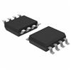
DescriptionThe MAX7302 features a port supply VLA that allows level-translation on I/O ports to operate from a separate power supply from 1.62V to 5.5V. An address select input, AD0, allows up to four unique slave addresses for the device. The MAX7302 includes an internal oscillator for PWM, blink, and key debounce, or to cascade multiple MAX7302s. The external clock can be used to set a specific PWM and blink timing. The RST input asynchronously clears the 2-wire interface and terminates a bus lockup involving the MAX7302. All ports configured as an output feature a 33-step PWM, allowing any output to be set from fully off, 1/32 to 31/32 duty cycle, to fully on. The MAX7302 I2C-/SMBus?-compatible, serial-interfaced peripheral features 9 level-translating I/Os, and operates from a 1.62V to 3.6V power supply. Ports P2-P9 can also be used as configurable logic arrays (CLAs)to form user-defined logic gates, replacing external discrete gates. Outputs are capable of sinking up to 25mA, and sourcing up to 10mA when configured as push-pull outputs. All output ports also feature LED blink control, allowing blink periods of 1/8s, 1/4s, 1/2s, 1s, 2s, 4s, or 8s. Any port can blink during this period with a 1/16 to 15/16 duty cycle. The MAX7302 is specified over the -40°C to +125°C temperature range and is available in 16-pin QSOP and 16-pin TQFN (3mm x 3mm)packages. The MAX7302 ports P2P9 can be configured as inputs, push-pull outputs, and open-drain outputs. Port P1 can be configured as a general-purpose input, open-drain output, or an open-drain INT output. Ports P2P9 can be configured as OSCIN and OSCOUT, respectively.
The features of MAX7302 can be summarized as (1)1.62V to 5.5V I/O level-translation port supply (VLA); (2)1.62V to 3.6V power supply; (3)9 individually configurable GPIO Ports P1 open-drain I/O P2P9 push-pull or open-drain I/Os; (4)individual 33-step PWM intensity control; (5)blink controls with 15 steps on outputs; (6)1kHz PWM period provides flicker-free LED intensity control; (7)25mA (max)port output sink current (100mA max Ground Current); (8)inputs overvoltage protected up to 5.5V (VLA); (9)transition detection with optional interrupt output; (10)optional input debouncing; (11)I/O ports configurable as logic gates (CLA); (12)external RST input; (13)oscillator input and output enable cascading multiple devices; (14)low 0.75A (typ)standby current.
The absolute maximum ratings of MAX7302 are (1)VDD: -0.3V to +4V; (2)VLA, SCL, SDA, AD0, RST, P1: -0.3V to +6V; (3)P2P9: -0.3V to VLA + 0.3V; (4)P1P9 sink current: 25mA; (5)P2P9 source current: 10mA; (6)SDA sink current: 10mA; (7)VDD current: 10mA; (8)VLA current: 35mA; (9)GND current: 100mA; (10)continuous power dissipation (TA = +70°C)16-Pin QSOP (derate 8.3mW/°C over +70°C): 666mW/ 16-Pin TQFN (derate 14.7mW/°C over +70°C): 1176mW; (11)operating temperature range: -40°C to +125°C; (12)junction temperature: +150°C; (13)storage temperature range: -65°C to +150°C; (14)lead temperature (soldering, 10s): +300°C.

 MAX7302 Data Sheet


