Features: HIGH SPEED fMAX =55 MHz (TYP.) AT VCC = 5 VLOWPOWER DISSIPATION ICC = 4 mA (MAX.) AT TA = 25 °CHIGH NOISE IMMUNITY VNIH = VNIL = 28 % VCC (MIN.)OUTPUT DRIVE CAPABILITY 15 LSTTL LOADS FOR QA TO QH 10 LSTTL LOADS FOR QH'SYMMETRICAL OUTPUT IMPEDANCE IOH| = IOL = 6 mA (MIN.) FOR QA TOQHIOH| ...
M74HC595: Features: HIGH SPEED fMAX =55 MHz (TYP.) AT VCC = 5 VLOWPOWER DISSIPATION ICC = 4 mA (MAX.) AT TA = 25 °CHIGH NOISE IMMUNITY VNIH = VNIL = 28 % VCC (MIN.)OUTPUT DRIVE CAPABILITY 15 LSTTL LOADS FOR Q...
SeekIC Buyer Protection PLUS - newly updated for 2013!
268 Transactions
All payment methods are secure and covered by SeekIC Buyer Protection PLUS.
HIGH SPEED fMAX = 55 MHz (TYP.) AT VCC = 5 V
LOWPOWER DISSIPATION ICC = 4 mA (MAX.) AT TA = 25 °C
HIGH NOISE IMMUNITY VNIH = VNIL = 28 % VCC (MIN.)
OUTPUT DRIVE CAPABILITY 15 LSTTL LOADS FOR QA TO QH 10 LSTTL LOADS FOR QH'
SYMMETRICAL OUTPUT IMPEDANCE
IOH| = IOL = 6 mA (MIN.) FOR QA TOQH
IOH| = IOL = 4 mA (MIN.) FOR QH'
BALANCEDPROPAGATION DELAYS tPLH = tPHL
WIDE OPERATING VOLTAGE RANGE VCC (OPR) = 2 V TO 6 V
PIN AND FUNCTION COMPATIBLE WITH 54/74LS595
Symbol |
Parameter |
Value |
Unit |
VCC |
Supply Voltage |
-0.5 to +7 |
V |
VI |
DC Input Voltage |
-0.5 to VCC + 0.5 |
V |
VO |
DC Output Voltage |
-0.5 to VCC + 0.5 |
V |
IIK |
DC Input Diode Current |
± 20 |
mA |
IOK |
DC Output Diode Current |
± 20 |
mA |
IO |
DC Output Current Per Output Pin QA-QH |
± 35 |
mA |
IO |
DC Output Current Per Output Pin QH' |
± 25 |
mA |
ICC or IGND |
DC VCC or Ground Current |
± 70 |
mA |
PD |
Power Dissipation |
500 (*) |
mW |
Tstg |
Storage Temperature |
-65 to +150 |
°C |
TL |
Lead Temperature (10 sec) |
300 |
°C |
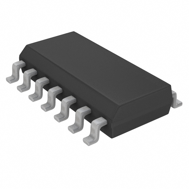
The M54/74HC595 is a high speed CMOS 8-BIT SHIFT REGISTERS/OUTPUT LATCHES (3- STATE) fabricated in silicon C2MOS technology. The M54/74HC595 has the same high speed performance of LSTTL combined with true CMOS low power consumption. This device contains an 8-bit serial-in, parallel-out shift register that feeds an 8-bit D-type storage register. The storage register has 8 3-STATE outputs. Separate clocks are provided for both the shift register and the storage register.
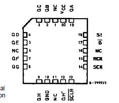
The shift register of M54/74HC595 has a direct-overriding clear, serial input, and serial output (standard) pins for cascading. Both the shift register and storage register use positive-edge triggered clocks. If both clocks are connected together, the shift register state will always be one clock pulse ahead of the storage register.
All inputs are equipped with protection circuits against static discharge and transient excess voltage.