Features: `LOW POWER DISSIPATION: ICC = 2A(MAX.) at TA=25°C`INJECTION CURRENT PROTECTION: VOUT<1mV at VCC=5V IIN1mA RS3.9K` ON RESISTANCE at TA=25°C: 215 TYP. (VCC = 3.0V) 150 TYP. (VCC = 4.5V) 160 TYP. (VCC = 6V)`FAST SWITCHING: tpd = 8.6ns (TYP.) at TA = 25 °C, VCC = 4.5V`WIDE OPERATING SUPPL...
M74HC4851: Features: `LOW POWER DISSIPATION: ICC = 2A(MAX.) at TA=25°C`INJECTION CURRENT PROTECTION: VOUT<1mV at VCC=5V IIN1mA RS3.9K` ON RESISTANCE at TA=25°C: 215 TYP. (VCC = 3.0V) 150 TYP. (VCC = 4.5V) 1...
SeekIC Buyer Protection PLUS - newly updated for 2013!
268 Transactions
All payment methods are secure and covered by SeekIC Buyer Protection PLUS.
Symbol | Parameter | Value | Unit | |
VCC | Supply Voltage | -0.5 to +7 | V | |
VI | DC Input Voltage | -0.5 to VCC + 0.5 | V | |
VO | DC Output Voltage | -0.5 to VCC + 0.5 | V | |
IIK | DC Input Diode Current | ± 20 | mA | |
IOK | DC Output Diode Current | ± 20 | mA | |
IO | DC Output Current | ± 25 | mA | |
ICC or IGND | DC VCC or Ground Current | ± 50 | mA | |
PD | Power Dissipation | SOP | 500(*) | mW |
TSSOP | 450(*) | mW | ||
Tstg | Storage Temperature | -65 to +150 | °C | |
TL | Lead Temperature (10 sec) | 300 | °C |
Absolute Maximum Ratings are those values beyond which damage to the device may occur. Functional operation under these conditions is not implied
(*) Power difssipation at 65 °C. Derating from 65°C to 125°C: SO Package -7mW/°C; TSSOP Package -6.1mW/°C
The M74HC4851 is a single eight-channel analog MULTIPLEXER/DEMULTIPLEXER fabricated with silicon gate C2MOS technology.
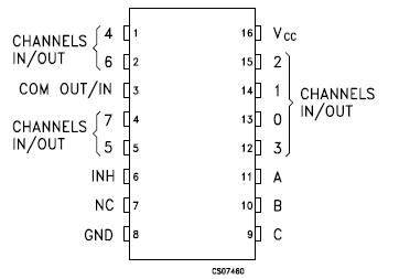
M74HC4851 is pin to pin compatible with the equivalent to standard HC4051 and MC14051, but feature injection current effect control. This make this device expecially suited for usage in automotive applications where voltages in excess of normal logic voltage are common. The injection current effect control of M74HC4851 allows signals at disabled input channels to exceed the supply voltage range or go down ground without affecting the signal of the enabled analog channel. This eliminated the need for external diode-resistor networks typically esed to keep the analog channel signals within the supply voltage range. This analog switch is bidirectional and digitally controlled. It have three binary control inputs A, B, abd C to select 1 of 8 to be turned on, and connected to the output, and a INH input to disable all channel.
All inputs and outputs are equipped with protection circuits against static discharge, giving them 2KV ESD immunity and transient excess voltage.