M66852FP

Features: • Memory configuration 64words x 9bits (M66850J/FP) 256words x 9bits (M66851J/FP) 512words x 9bits (M66852J/FP) 1024words x 9bits (M66853J/FP)• Write and Read Clocks can be independent• Advanced CMOS technology• Programmable Almost-Empty and Almost-Full flags̶...

product image

M66852FP Picture
SeekIC No. : 004406912 Detail

M66852FP: Features: • Memory configuration 64words x 9bits (M66850J/FP) 256words x 9bits (M66851J/FP) 512words x 9bits (M66852J/FP) 1024words x 9bits (M66853J/FP)• Write and Read Clocks can be ind...

floor Price/Ceiling Price

Part Number:
M66852FP
Supply Ability:
5000

Price Break

  • Qty
  • 1~5000
  • Unit Price
  • Negotiable
  • Processing time
  • 15 Days
Total Cost: $ 0.00

SeekIC Buyer Protection PLUS - newly updated for 2013!

  • Escrow Protection.
  • Guaranteed refunds.
  • Secure payments.
  • Learn more >>

Month Sales

268 Transactions

Rating

evaluate  (4.8 stars)

Upload time: 2024/11/27

Payment Methods

All payment methods are secure and covered by SeekIC Buyer Protection PLUS.

Notice: When you place an order, your payment is made to SeekIC and not to your seller. SeekIC only pays the seller after confirming you have received your order. We will also never share your payment details with your seller.
Product Details

Description


Features:

• Memory configuration 64words x 9bits (M66850J/FP) 256words x 9bits (M66851J/FP) 512words x 9bits (M66852J/FP) 1024words x 9bits (M66853J/FP)
• Write and Read Clocks can be independent
• Advanced CMOS technology
• Programmable Almost-Empty and Almost-Full flags
• High-speed : 25ns cycle time
• Package Available : 32-pin Pastic Leaded Chip Carrier(PLCC) 32-pin Low profile Quad Flat Package(LQFP)


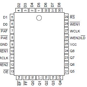
Pinout

  Connection Diagram


Specifications

Symbol Parameter Conditions Ratings Unit
Vcc Supply voltage   -0.5 +7.0 V
VI Input voltage -0.3 VCC+0.5 V
VO Output voltage -0.3 VCC+0.5 V
Pd Maximum power dissipation Ta=70°C Note mW
Tstg Storage temperature   -65 150


Description

M66850/851/852/853 are very high-speed and clock synchronous FIFO(First-In,First-Out) memories fabricated by high-speed CMOS technology.

These M66850/851/852/853 are applicable for a data buffer as networks and communications.

The write operation is controlled by a write clock pin(WCLK) and two write enable pins(WEN1WEN2 ).

Data present at the data input pins(D0-D8) is written into the Synchronous FIFO on every rising write clock edge when the device is enabled for writing.

The read operation is controlled by a read clock pin(RCLK) and two read enable pins(REN1,REN2).

Data is read from the Synchronous M66850/851/852/853 on every rising read clock edge when the device is enabled for reading. An output enable pin(OE) controls the states of the data output pins(Q0-Q8).

MITSUBISHI FIFOs have four flags (EF,FF,PAE,PAF). The empty flag EF and the full flag FF are fixed flags. The almost empty flag PAE and the almost full flag PAF are programmable flags. The programmable flag offset is initiated by the load pin(LD).


Customers Who Bought This Item Also Bought

Margin,quality,low-cost products with low minimum orders. Secure your online payments with SeekIC Buyer Protection.
Transformers
Hardware, Fasteners, Accessories
Crystals and Oscillators
Cables, Wires
Resistors
Optical Inspection Equipment
View more