M58WT032KT

Features: ` Supply voltage VDD = 1.7 V to 2 V for program, erase and read VDDQ = 2.7 V to 3.3 V for I/O buffers VPP = 9 V for fast program` Synchronous/asynchronous read Synchronous burst read mode: 52 MHz Asynchronous/synchronous page read mode Random access times: 70 ns` Synchronous burst rea...

product image

M58WT032KT Picture
SeekIC No. : 004406150 Detail

M58WT032KT: Features: ` Supply voltage VDD = 1.7 V to 2 V for program, erase and read VDDQ = 2.7 V to 3.3 V for I/O buffers VPP = 9 V for fast program` Synchronous/asynchronous read Synchronous burst read mod...

floor Price/Ceiling Price

Part Number:
M58WT032KT
Supply Ability:
5000

Price Break

  • Qty
  • 1~5000
  • Unit Price
  • Negotiable
  • Processing time
  • 15 Days
Total Cost: $ 0.00

SeekIC Buyer Protection PLUS - newly updated for 2013!

  • Escrow Protection.
  • Guaranteed refunds.
  • Secure payments.
  • Learn more >>

Month Sales

268 Transactions

Rating

evaluate  (4.8 stars)

Upload time: 2024/11/27

Payment Methods

All payment methods are secure and covered by SeekIC Buyer Protection PLUS.

Notice: When you place an order, your payment is made to SeekIC and not to your seller. SeekIC only pays the seller after confirming you have received your order. We will also never share your payment details with your seller.
Product Details

Description


Features:

` Supply voltage
VDD = 1.7 V to 2 V for program, erase and read
VDDQ = 2.7 V to 3.3 V for I/O buffers
VPP = 9 V for fast program
` Synchronous/asynchronous read
Synchronous burst read mode: 52 MHz
Asynchronous/synchronous page read mode
Random access times: 70 ns
` Synchronous burst read suspend
` Programming time
10 s by word typical for fast factory program
Double/quadruple word program option
Enhanced factory program options
` Memory blocks
Multiple bank memory array: 4 Mbit banks
Parameter blocks (top or bottom location)
` Dual operations
Program erase in one bank while read in others
No delay between read and write
  operations
` Block locking
All blocks locked at power-up
Any combination of blocks can be locked
WP for block lock-down
` Security
128-bit user programmable OTP cells
64-bit unique device number
` Common Flash interface (CFI)
` 100 000 program/erase cycles per block
` Electronic signature
Manufacturer code: 20h
Device codes:
  M58WT032KT (top): 8866h
  M58WT032KB (bottom): 8867h
M58WT064KT (top): 8810h
  M58WT064KB (bottom): 8811h
` ECOPACK® package available


Pinout

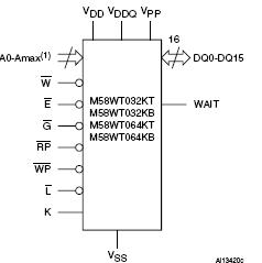
  Connection Diagram


Specifications

Symbol Parameter Value Unit
Min Max
TA Ambient Operating Temperature (1) -40 85 °C
TBIAS Temperature Under Bias -40 125 °C
TSTG Storage Temperature -65 155 °C
VIO Input or Output Voltage -0.5 VDDQ+0.6 V
VDD, Supply Voltage -0.2 2.45 V
VDDQ Input/output supply voltage -0.2 3.6 V
VPP Program Voltage -0.2 10 V
Io Output short circuit current   100 mA
tVPPH Time for VPP at VPPH   100 hours


Description

The M58WT032KT/B and M58WT064KT/B are 32 Mbit (2 Mbit *16) and 64 Mbit (4 Mbit *16) non-volatile Flash memories, respectively. They can be erased electrically at block level and programmed in-system on a word-by-word basis using a 1.7 V to 2 V VDD supply for the circuitry and a 2.7 V to 3.3 V VDDQ supply for the input/output pins. An optional 9 V VPP power supply is provided to speed up customer programming.

M58WTxxxKT/B is the collective name for all these devices. They feature an asymmetrical block architecture.
The M58WT032KT/B has an array of 71 blocks, and is divided into 4 Mbit banks. There are 7 banks each containing 8 main blocks of 32 Kwords, and one parameter bank containing 8 parameter blocks of 4 Kwords and 7 main blocks of 32 Kwords.

The M58WT064KT/B has an array of 135 blocks, and is divided into 4 Mbit banks. There are 15 banks each containing 8 main blocks of 32 Kwords, and one parameter bank containing 8 parameter blocks of 4 Kwords and 7 main blocks of 32 Kwords.

The M58WT032KT/B and M58WT064KT/B multiple bank architecture allows dual operations. While programming or erasing in one bank, read operations are possible in other banks. Only one bank at a time is allowed to be in program or erase mode. It is possible to perform burst reads that cross bank boundaries. The bank architectures are summarized in Table 2 and Table 3 and the memory maps are shown in Figure 3 and Figure 4. The parameter blocks are located at the top of the memory address space for the M58WT032KT and M58WT064KT, and at the bottom for the M58WT032KB and M58WT064KB.

Each block can be erased separately. Erase can be suspended to perform program in any other block, and then resumed. Program can be suspended to read data in any other block and then resumed. Each block can be programmed and erased over 100 000 cycles using the supply voltage VDD. Two enhanced factory programming commands are available to speed up programming.

Program and erase commands are written to the command interface of the memory. An internal Program/Erase Controller manages the timings necessary for program and erase operations. The end of a program or erase operation can be detected and any error conditions identified in the Status Register. The command set required to control the memory is consistent with JEDEC standards.

The device supports synchronous burst read and asynchronous read from all blocks of the memory array; at power-up the device is configured for asynchronous read. In synchronous burst mode, data is output on each clock cycle at frequencies of up to 52 MHz. The synchronous burst read operation can be suspended and resumed.

The device features an automatic standby mode. When the bus is inactive during asynchronous read operations, the device automatically switches to the automatic standby mode. In this condition the power consumption is reduced to the standby value IDD4 and the outputs are still driven.


Customers Who Bought This Item Also Bought

Margin,quality,low-cost products with low minimum orders. Secure your online payments with SeekIC Buyer Protection.