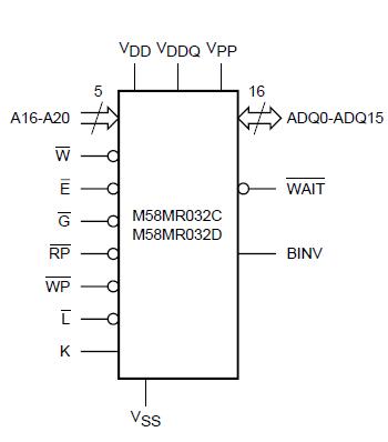
Features: SUPPLY VOLTAGE
VDD = VDDQ = 1.7V to 2.0V for Program, Erase and Read
VPP = 12V for fast Program (optional)
MULTIPLEXED ADDRESS/DATA
SYNCHRONOUS / ASYNCHRONOUS READ
Burst mode Read: 40MHz
Page mode Read (4 Words Page)
Random Access: 100ns
PROGRAMMING TIME
10s by Word typical
Two or four words programming option
MEMORY BLOCKS
Dual Bank Memory Array: 8/24 Mbit
Parameter Blocks (Top or Bottom location)
DUAL OPERATIONS
Read within one Bank while Program or Erase within the other
No delay between Read and Write operations
PROTECTION/SECURITY
All Blocks protected at Power-up
Any combination of Blocks can be protected
64 bit unique device identifier
64 bit user programmable OTP cells
One parameter block permanently lockable
COMMON FLASH INTERFACE (CFI)
100,000 PROGRAM/ERASE CYCLES per BLOCK
ELECTRONIC SIGNATURE
Manufacturer Code: 20h
Top Device Code, M58MR032C: 88DAh
Bottom Device Code, M58MR032D: 88DBhPinout Specifications
|
Symbol |
Parameter |
Value |
Unit |
|
TA |
Ambient Operating Temperature (2) |
40 to 85 |
°C |
|
TBIAS |
Temperature Under Bias |
40 to 125 |
°C |
|
TBIAS |
Storage Temperature |
55 to 155 |
°C |
|
VIO(3) |
Input or Output Voltage |
0.5 to VDDQ+0.5 |
V |
|
VDD, VDDQ |
Supply Voltage |
0.5 to 2.7 |
V |
|
VPP |
Program Voltage |
0.5 to 13 |
V |
Note: 1. Except for the rating "Operating Temperature Range", stresses above those listed in the Table "Absolute Maximum Ratings" may cause permanent damage to the device. These are stress ratings only and operation of the device at these or any other conditions above those indicated in the Operating sections of this specification is not implied. Exposure to Absolute Maximum Rating conditions for extended periods may affect device reliability. Refer also to the STMicroelectronics SURE Program and other relevant quality documents.
2. Depends on range.
3. Minimum Voltage may undershoot to 2V during transition and for less than 20ns.
DescriptionThe M58MR032 is a 32 Mbit non-volatile Flash memory that may be erased electrically at block level and programmed in-system on a Word-by- Word basis using a 1.7V to 2.0V VDD supply for the circuitry. For Program and Erase operations the necessary high voltages are generated internally. The device supports synchronous burst read and asynchronous read from all the blocks of the memory array; at power-up the device is configured for page mode read. In synchronous burst mode, a new data is output at each clock cycle for frequencies up to 40MHz.
The M58MR032 array matrix organization allows each block to be erased and reprogrammed without affecting other blocks. All blocks are protected against programming and erase at Power-up. Blocks can be unprotected to make changes in the application and then re-protected.
M58MR032 A parameter block "Security block" can be permanently protected against programming and erasing in order to increase the data security. An optional 12V VPP power supply is provided to speed up the program phase at costumer production. An internal command interface (C.I.) decodes the instructions to access/modify the memory content. The program/erase controller (P/E.C.) automatically executes the algorithms taking care of the timings necessary for program and erase operations. Two status registers indicate the state of each bank.
M58MR032 Instructions for Read Array, Read Electronic Signature, Read Status Register, Clear Status Register, Write Read Configuration Register, Program, Block Erase, Bank Erase, Program Suspend, Program Resume, Erase Suspend, Erase Resume, Block Protect, Block Unprotect, Block Locking, Protection Program, CFI Query, are written to the memory through a Command Interface (C.I.) using standard micro-processor write timings.
The M58MR032 memory is offered in TFBGA48, 0.5 mm ball pitch packages and it is supplied with all the bits erased (set to '1').

 M58MR032C Data Sheet


