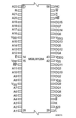
Features: WIDE DATA BUS for HIGH BANDWIDTH M58LW128A: x16 M58LW128B: x16/x32 SUPPLY VOLTAGE VDD = 2.7 to 3.6V core supply voltage for Program, Erase and Read operations VDDQ = 1.8 to VDD for I/O Buffers SYNCHRONOUS/ASYNCHRONOUS READ Synchronous Burst read Pipelined Synchronous Burst Read Asynchro...
M58LW128A: Features: WIDE DATA BUS for HIGH BANDWIDTH M58LW128A: x16 M58LW128B: x16/x32 SUPPLY VOLTAGE VDD = 2.7 to 3.6V core supply voltage for Program, Erase and Read operations VDDQ = 1.8 to VDD for I/O Bu...
SeekIC Buyer Protection PLUS - newly updated for 2013!
268 Transactions
All payment methods are secure and covered by SeekIC Buyer Protection PLUS.
Features: SUPPLY VOLTAGE VDD = 1.7V to 2.0V for program, erase and read VDDQ = 1.7V to 2.0V for I...
Features: Supply voltage VDD = 1.7 V to 2.0 V for program, erase and read VDDQ = 1.7 V to 2.0 V f...
Symbol |
Parameter |
Value |
Unit | |
Min |
Max | |||
TBIAS |
Temperature Under Bias |
40 |
125 |
°C |
TSTG |
Storage Temperature |
55 |
150 |
°C |
TLEAD |
Maximum TLEAD Temperature during soldering |
t.b.a. |
°C | |
VIO |
Input or Output Voltage |
0.6 |
VDDQ +0.6 |
V |
VDD, VDDQ |
Supply Voltage |
0.6 |
5.0 |
V |
VHH |
RP Hardware Block Unprotect Voltage |
0.6 |
100(1) |
V |
M58LW128 is a 128 Mbit (8Mb x16 or 4Mb x32) non-volatile memory that can be read, erased and reprogrammed. These operations can be performed using a single low voltage (2.7V to 3.6V) core supply. On power-up the memory defaults to Read mode with an asynchronous bus where it can be read in the same way as a non-burst Flash memory.
The memory of M58LW128 is divided into 128 blocks of 1Mbit that can be erased independently so it is possible to preserve valid data while old data is erased. Program and Erase commands are written to the Command Interface of the memory. An on-chip Program/Erase Controller simplifies the process of programming or erasing the memory by taking care of all of the special operations that are required to update the memory contents. The end of a Program or Erase operation can be detected and any error conditions identified in the Status Register. The command set required to control the memory is consistent with JEDEC standards.
The Write Buffer of M58LW128 allows the microprocessor to program up to 16 Words (or 8 Double Words) in parallel, both speeding up the programming and freeing up the microprocessor to perform other work. The minimum buffer size for a program operation is an 8 Word (or 4 Double Word) page. A page can only be programmed once between Erase operations.
Erase can be suspended in order to perform either read or program in any other block and then resumed. Program can be suspended to read data in any other block and then resumed. Each block can be programmed and erased over 100,000 cycles.
Individual block protection against program or erase is provided for data security. All blocks are protected during power-up. The protection of the blocks is non-volatile; after power-up the protection status of each block is restored to the state when power was last removed. Software commands are provided to allow protection of some or all of the blocks and to cancel all block protection bits simultaneously. All program or erase operations are blocked when the Program Erase Enable input Vpp is low.
The Reset/Power-Down pin of M58LW128 is used to apply a Hardware Reset to the memory and to set the device in Power-Down mode. It can also be used to temporarily disable the protection mechanism. In asynchronous mode Chip Enable, Output Enable and Write Enable signals control the bus operation of the memory. An Address Latch input can be used to latch addresses in Latch Controlled mode. Together they allow simple, yet powerful, connection to most microprocessors, often without additional logic.
In synchronous mode all Bus Read operations are synchronous with the Clock. Chip Enable and Output Enable select the Bus Read operation; the address is Latched using the Latch Enable inputs and the address is advanced using Burst Address Advance. The signals are compatible with most microprocessor burst interfaces.
A One Time Programmable (OTP) area is included for security purposes. Either 512 Words (x16 Bus Width) or 512 Double-Words (x32 Bus Width) is available in the OTP area. The process of reading from and writing to the OTP area is not published for security purposes; contact STMicroelectronics for details on how to use the OTP area.
The memory of M58LW128 is offered in various packages. The M58LW128A is available in TSOP56 (14 x 20 mm) and TBGA64 (1mm pitch). The M58LW128B is available in TBGA80 (1mm pitch).