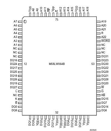
M58LW064B

PinoutSpecifications Symbol Parameter Value Unit TA Ambient Operating Temperature Grade 1 0 to 70 °C Grade 6 40 to 85 TBIAS Temperature Under Bias 40 to 125 °C TSTG Storage Temperature 55 to 150 °C VIO Input or Output Voltage 0.6 ...

product image

M58LW064B Picture
SeekIC No. : 004406123 Detail

M58LW064B: PinoutSpecifications Symbol Parameter Value Unit TA Ambient Operating Temperature Grade 1 0 to 70 °C Grade 6 40 to 85 TBIAS Temperature Under Bias 40 to 1...

floor Price/Ceiling Price

Part Number:
M58LW064B
Supply Ability:
5000

Price Break

  • Qty
  • 1~5000
  • Unit Price
  • Negotiable
  • Processing time
  • 15 Days
Total Cost: $ 0.00

SeekIC Buyer Protection PLUS - newly updated for 2013!

  • Escrow Protection.
  • Guaranteed refunds.
  • Secure payments.
  • Learn more >>

Month Sales

268 Transactions

Rating

evaluate  (4.8 stars)

Upload time: 2024/11/27

Payment Methods

All payment methods are secure and covered by SeekIC Buyer Protection PLUS.

Notice: When you place an order, your payment is made to SeekIC and not to your seller. SeekIC only pays the seller after confirming you have received your order. We will also never share your payment details with your seller.
Product Details

Description


Pinout

  Connection Diagram


Specifications

Symbol
Parameter
Value
Unit
TA
Ambient Operating Temperature Grade 1
0 to 70
°C
Grade 6 40 to 85  
TBIAS
Temperature Under Bias
40 to 125
°C
TSTG
Storage Temperature
55 to 150
°C
VIO
Input or Output Voltage
0.6 to VDDQ +0.6
V
VDD, VDDQ
Supply Voltage
0.6 to 5.0
V
VHH
RP Hardware Block Unlock Voltage
0.6 to 10 (2)
V


Description

The M58LW064 is a non-volatile Flash memory that may be erased electrically at the block level and programmed in-system on a 16 Word or 8 m Double-Word basis using a 2.7V to 3.6V supply for the circuit and a supply down to 1.8V for the Input and Output buffers. The M58LW064A is organised as 4M by 16 bit. The M58LW064B has 4M by 16m bit or 2M by 32 bit organisation selectable by the Word Organisation WORD input. Both devices are internally configured as 64 blocks of 1 Mbit each.

The M58LW064B support Asynchronous Random and Latch Enable Controlled Read with Page mode as well as Synchronous Burst Read with a configurablem burst. They also support pipelined synchronous Burst Read. Writing is Asynchronous or Asynchronous Latch Enable Controlled.

The configurable synchronous burst read interface of M58LW064B allows a high data transfer rate controlled by the Burst Clock K signal. It is capable of bursting fixed or unlimited lengths of data. The burst type, latency and length are configurable and can be easily adapted to a large variety of system clock frequencies and microprocessors. A 16 Word or 8 Double- Word Write Buffer improves effective programming speed by up to 20 times when data is programmed in full buffer increments. Effective Word programming takes typically 12ms. The array matrix organisation allows each block to be erased and reprogrammed without affecting other blocks.

Program and Erase operations of M58LW064B can be suspended in order to perform either Read or Program in any other block and then resumed. All blocks are protected against spurious programming and erase cycles at power-up. Any block can be separately protected at any time. The block protection bits can also be deleted, this is executed as one sequence for all blocks simultaneously. Block protection can be temporarily disabled. Each block can be programmed and erased over 100,000 cycles. Block erase is performed in typically 1 second.

An internal Command Interface (C.I.) decodes Instructions to access/modify the memory content. The Program/Erase Controller (P/E.C.) automatically executes the algorithms taking care of the timings required by the program and erase operations. Verification is internally performed and a Status Register tracks the status of the operations. The Ready/Busy output RB indicates the completion of operations.

Instructions of M58LW064B are written to the memory through the Command Interface (C.I.) using standard microprocessor write timings. The device supports the Common Flash Interface (CFI) command set definition.

A Reset/Power-down mode is entered when the RP input is Low. In this mode the power consumption is lower than in the normal standby mode, the device is write protected and both the Status and the Burst Configuration Registers are cleared. A recovery time is required when the RP input goes High.

The device is offered in various package versions, TSOP56 (14 x 20 mm), TSOP86 Type II (11.76 x 22.22 mm) and LBGA54 1mm ball pitch for the M58LW064A and PQFP80 for the M58LW064B.


Customers Who Bought This Item Also Bought

Margin,quality,low-cost products with low minimum orders. Secure your online payments with SeekIC Buyer Protection.
Optoelectronics
Semiconductor Modules
RF and RFID
Optical Inspection Equipment
Test Equipment
Computers, Office - Components, Accessories
View more