Features: Supply voltage
VDD = 2.7 V to 3.6 V for program, erase and read
VDDQ = VDDQIN = 2.4 V to 3.6 V for I/O buffers
VPP = 12 V for fast program (optional)
High performance
Access times: 70, 80 ns
56 MHz effective zero wait-state burst read
Synchronous burst read
Asynchronous page read
Hardware block protection
WP pin for write protect of the 4 outermost parameter blocks and all main blocks
RP pin for write protect of all blocks
Optimized for FDI drivers
Fast program / erase suspend latency time < 6 µs
Common Flash interface
Memory blocks
8 parameters blocks (top or bottom)
31 main blocks
Low power consumption
5 µA typical deep power-down
60 µA typical standby for M58BW016DT/B 150 µA typical standby for M58BW016FT/B
Automatic standby after asynchronous read
Electronic signature
Manufacturer code: 20h
Top device code: 8836h
Bottom device code: 8835h
100 K write/erase cycling + 20 years data retention (minimum)
High reliability level with over 1 M write/erase cycling sustained
ECOPACK® packages availablePinout Specifications
| Symbol |
Parameter |
Value |
Unit |
| Min |
Max |
| TBIAS |
Temperature under bias |
40 |
125 |
°C |
| TSTG |
Storage temperature |
55 |
155 |
°C |
| VIO |
Input or output voltage |
0.6 |
VDDQ + 0.6
VDDQIN + 0.6 |
V |
| VDD, VDDQ, VDDQIN |
Supply voltage |
0.6 |
4.2 |
V |
| VPP |
Program voltage |
0.6 |
13.5(1) |
V |
Stressing the device above the ratings listed in Table 12: Absolute maximum ratings, may cause permanent damage to the device. These are stress ratings only and operation of the device at these or any other conditions above those indicated in the operating sections of this specification is not implied. Exposure to absolute maximum rating conditions for extended periods may affect device reliability. Refer also to the Numonyx SURE Program and other relevant quality documents.
DescriptionThe M58BW016DT, M58BW016DB, M58BW016FT and M58BW016FB are 16-Mbit nonvolatile Flash memories that can be erased electrically at the block level and programmed in-system on a double-word basis using a 2.7 V to 3.6 V VDD supply for the circuit and a VDDQ supply down to 2.4 V for the input and output buffers. Optionally a 12 V VPP supply can be used to provide fast program and erase for a limited time and number of program/erase cycles.
The devices M58BW016DT, M58BW016DB, M58BW016FT and M58BW016FB support asynchronous (latch controlled and page read) and synchronous bus operations. The synchronous burst read interface allows a high data transfer rate controlled by the burst clock, K, signal. It is capable of bursting fixed or unlimited lengths of data. The burst type, latency and length can be configured and can be easily adapted to a large variety of system clock frequencies and microprocessors. All writes are asynchronous. On power-up the memory defaults to read mode with an asynchronous bus.
The devices M58BW016DT, M58BW016DB, M58BW016FT and M58BW016FB have a boot block architecture with an array of 8 parameter blocks of 64 Kbits each and 31 main blocks of 512 Kbits each. In the M58BW016DT and M58BW016FT the parameter blocks are located at the top of the address space whereas in the M58BW016DB and M58BW016FB, they are located at the bottom.
M58BW016DT, M58BW016DB, M58BW016FT and M58BW016FB Program and erase commands are written to the command interface of the memory. An onchip program/erase controller simplifies the process of programming or erasing the memory by taking care of all of the special operations that are required to update the memory contents. The end of a program or erase operation can be detected and any error conditions identified in the status register. The command set required to control the memory is consistent with JEDEC standards.
M58BW016DT, M58BW016DB, M58BW016FT and M58BW016FB Erase can be suspended in order to perform either read or program in any other block and then resumed. Program can be suspended to read data in any other block and then resumed. Each block can be programmed and erased over 100,000 cycles.
M58BW016DT, M58BW016DB, M58BW016FT and M58BW016FB All blocks are protected during power-up.
The M58BW016DT, M58BW016DB, M58BW016FT and M58BW016FB feature two different levels of block protection to avoid unwanted program/erase operations:
The WP pin offers an hardware protection on two of the parameter blocks and all of the main blocks
All program or erase operations are blocked when Reset, RP, is held Low. A reset/power-down mode is entered when the RP input is Low. In this mode the power consumption is lower than in the normal standby mode, the device is write protected and both the status and the burst configuration registers are cleared. A recovery time is required when the RP input goes High.
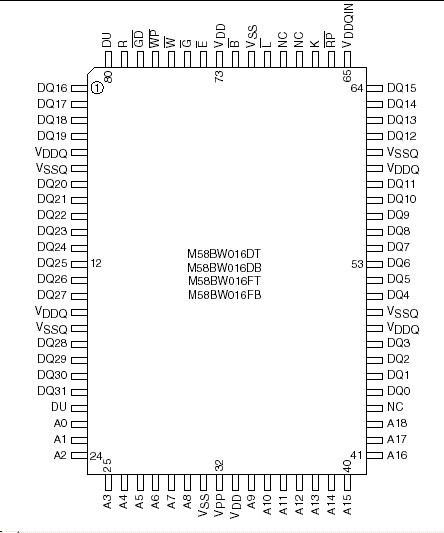
The memory is offered in a PQFP80 (14 x 20 mm) and LBGA80 (10 * 12 mm) package.
The memories are supplied with all the bits erased (set to '1').
In the present document, M58BW016DT, M58BW016DB, M58BW016FT and M58BW016FB will be referred to as M58BW016 unless otherwise specified.

 M58BW016FB Data Sheet


