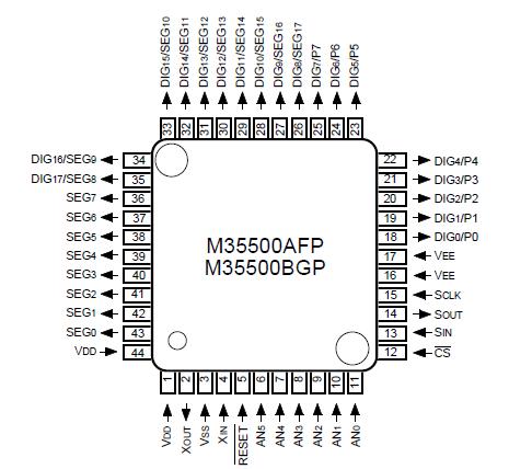
Features: • High-breakdown-voltage output port ...................................26• Segment output..............................................................8 to 18• Digit output ....................................................................7 to 10 (Ports P0 to P2 are ...
M35500AFP: Features: • High-breakdown-voltage output port ...................................26• Segment output..............................................................8 to 18• Digit out...
SeekIC Buyer Protection PLUS - newly updated for 2013!
268 Transactions
All payment methods are secure and covered by SeekIC Buyer Protection PLUS.
Symbol |
Parameter |
Conditions |
Ratings |
Unit |
VCC | Power source voltage | • All voltage are based on VSS. |
0.3 to 6.5 |
V |
VEE | Pull-down power source voltage | • Output transistors are cut off. |
VCC45 to VCC+0.3 |
V |
VI | Input voltage AN0 AN5 |
0.3 to VCC+0.3 |
V | |
VI | Input voltage CS, SIN, SCLK |
0.3 to VCC+0.3 |
V | |
VI | Input voltage RESET |
0.3 to VCC+0.3 |
V | |
VO | Input voltage __ DIG0 DIG17 SEG0 SEG17 |
VCC45 to VCC+0.3 |
V | |
• All voltage are based on VSS. • Output transistors are cut off. • A waveform: 450 ms or more frequency and 30 ms or less pulse width. • Connect only capacitor load (CL = 200pF). |
VCC50 to VCC+0.3 |
V | ||
VO | Output voltage SOUT | • All voltage are based on VSS. • Output transistors are cut off. |
0.3 to VCC+0.3 |
|
Pd | Power dissipation | Ta = 25 |
600 |
mW |
Topr | Operating temperature |
20 to 85 |
| |
Tstg | Storage temperature |
40 to 125 |
|