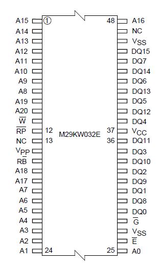
Features: SUPPLY VOLTAGE VCC = 2.7V to 3.6V for Read VPP = 11.4V to 12.6V for Program and Erase ACCESS TIME: 90, 110ns PROGRAMMING TIME 9s per Word typical Multiple Word Programming Option (4s typical Chip Program) ERASE TIME 21s typical factory Chip Erase UNIFORM BLOCKS 16 blocks of 2 Mbit...
M29KW032E: Features: SUPPLY VOLTAGE VCC = 2.7V to 3.6V for Read VPP = 11.4V to 12.6V for Program and Erase ACCESS TIME: 90, 110ns PROGRAMMING TIME 9s per Word typical Multiple Word Programming Option (4s ...
SeekIC Buyer Protection PLUS - newly updated for 2013!
268 Transactions
All payment methods are secure and covered by SeekIC Buyer Protection PLUS.
Symbol |
Parameter |
Min |
Max |
Unit |
TBIAS |
Temperature Under Bias |
50 |
125 |
°C |
TSTG |
Storage Temperature |
65 |
150 |
°C |
VIO |
Input or Output Voltage(1,2) |
0.6 |
VCC +0.6 |
V |
VCC |
Read Supply Voltage |
0.6 |
4 |
V |
Vpp |
Program/Erase Supply Voltage |
0.6 |
13.5 |
V |
The M29KW032E LightFlash™ is a 32 Mbit (2Mb x16) non-volatile memory that can be read, erased and reprogrammed. Read operations can be performed using a single low voltage (2.7 to 3.6V) supply. Program and Erase operations require an additional VPP (11.4 to 12.6) power supply. On power-up the memory defaults to its Read mode where it can be read in the same way as a ROM or EPROM.
The memory M29KW032E is divided into 16 uniform blocks that can be erased independently so it is possible to preserve valid data while old data is erased (see Figures 2, Block Addresses). Program and Erase commands are written to the Command Interface of the memory. An on-chip Program/Erase Controller (P/E.C.) simplifies the process of programming or erasing the memory by taking care of all of the special operations that are required to update the memory contents.
The M29KW032E LightFlash™ features a new command, Multiple Word Program, used to program large streams of data. It greatly reduces the total programming time when a large number of Words are written to the memory at any one time. Using this command the entire memory can be programmed in 2s, compared to 9s using the standard Word Program.
The end of a program or erase operation M29KW032E can be detected and any error conditions identified. The command set required to control the memory is consistent with JEDEC standards. Chip Enable, Output Enable and Write Enable signals control the bus operation of the memory. They allow simple connection to most microprocessors, often without additional logic.
The memory is offered in TSOP48 (12 x 20mm) and TFBGA48 (6 x 9mm, 0.8mm pitch) packages. The memory is supplied with all the bits erased (set to '1').