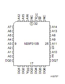
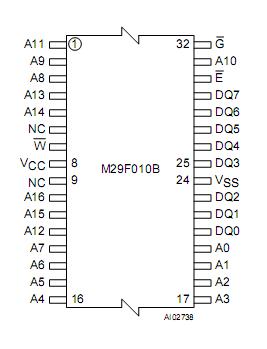
Features: SINGLE 5V±10% SUPPLY VOLTAGE for PROGRAM, ERASE and READ OPERATIONS
ACCESS TIME: 45ns
PROGRAMMING TIME8µs per Byte typical
8 UNIFORM 16 KBytes MEMORY BLOCKS
PROGRAM/ERASE CONTROLLER
Embedded Byte Program algorithm
Embedded Multi-Block/Chip Erase algorithm
Status Register Polling and Toggle Bits
ERASE SUSPEND and RESUME MODES
Read and Program another Block duringErase Suspend
UNLOCK BYPASS PROGRAM COMMAND
Faster Production/Batch Programming
LOW POWER CONSUMPTION
Standby and Automatic Standby
100,000 PROGRAM/ERASE CYCLES per BLOCK
20 YEARS DATA RETENTION
Defectivity below 1 ppm/year
ELECTRONIC SIGNATURE
Manufacturer Code: 20h
Device Code: 20h
ECOPACK®PACKAGES AVAILABLEPinout
 Specifications
| Symbol |
Parameter |
Value |
Unit |
| T A |
Ambient Operating Temperature (Temperature Range Option 1) |
0 to 70 |
°C |
| Ambient Operating Temperature (Temperature Range Option 6) |
40 to 85 |
°C |
| Ambient Operating Temperature (Temperature Range Option 3) |
40 to 125 |
°C |
| T BIAS |
Temperature Under Bias |
50 to 125 |
°C |
| T STG |
Storage Temperature |
65 to 150 |
°C |
| V IO (2) |
Input or Output Voltage |
0.6 to 6 |
V |
| V CC |
Supply Voltage |
0.6 to 6 |
V |
| V ID |
Identification Voltage |
0.6 to 13.5 |
V |
DescriptionThe M29F010B is a 1 Mbit (128Kb x8) non-volatilememory that can be read, erased and repro-grammed. These operations can be performed us-ing a single 5V supply. On power-up the memorydefaults to its Read mode where it can be read inthe same way as a ROM or EPROM.
The memory M29F010B is divided into blocks that can beerased independently so it is possible to preservevalid data while old data is erased. Each block can be protected independently to prevent accidental Program or Erase commands from modifying the memory. Program and Erase commands are writ-ten to the Command Interface of the memory. Anon-chip Program/Erase Controller simplifies theprocess of programming or erasing the memory by taking care of all of the special operations that are required to update the memory contents. The end of a program or erase operation can be detected and any error conditions identified. The command set required to control the memory is consistent with JEDEC standards.
Chip Enable, Output Enable and Write Enable sig-nals control the bus operation of the memory.They allow simple connection to most micropro-c essors, often without additional logic. The memory is offered in PLCC32, TSOP32 (8 x20mm) packages and it is supplied with all the bits erased (set to '1').In order to meet environmental requirements, SToffers the M29F010B in ECOPACK®packages.
ECOPACK packages are Lead-free. The category of second Level Interconnect is marked on the package and on the inner box label, in compliance with JEDEC Standard JESD97.

 M29F010B Data Sheet


