Features: `SUPPLY VOLTAGE
VCC = 2.7V to 3.6V for Program, Erase and Read
VPP =12V for Fast Program (optional)
`ASYNCHRONOUS PAGE READ MODE
Page Width 4 Words
Page Access 25, 30ns
Random Access 70, 90ns
`PROGRAMMING TIME
10µs per Byte/Word typical
4 Words / 8 Bytes at-a-time Program
`MEMORY BLOCKS
Quadruple Bank Memory Array: 8Mbit+24Mbit+24Mbit+8Mbit
Parameter Blocks (at both Top and Bottom)
`DUAL OPERATIONS
While Program or Erase in a group of banks (from 1 to 3), Read in any of the other banks
`PROGRAM/ ERASE SUSPEND and RESUME MODES
Read from any Block during Program Suspend
Read and Program another Block during Erase Suspend
`UNLOCK BYPASS PROGRAM COMMAND
Faster Production/Batch Programming
`VPP/WP PIN for FAST PROGRAM and WRITE PROTECT
`TEMPORARY BLOCK UNPROTECTION MODE
`COMMON FLASH INTERFACE
64 bit Security Code
`EXTENDED MEMORY BLOCK
Extra block used as security block or to store additional information
`LOW POWER CONSUMPTION
Standby and Automatic Standby
`100,000 PROGRAM/ERASE CYCLES per BLOCK
`ELECTRONIC SIGNATURE
Manufacturer Code: 0020h
Device Code: 227Eh + 2202h + 2201hPinout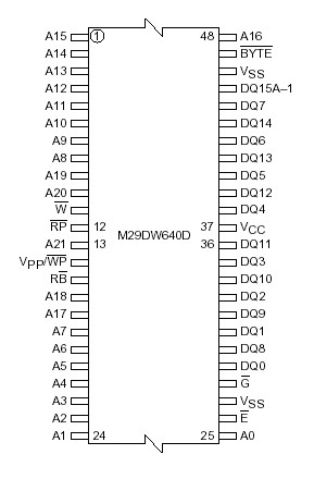 Specifications
| Symbol |
Parameter |
Min |
Max |
Unit |
| TBIAS |
Temperature Under Bias |
50 |
125 |
|
| TSTG |
Storage Temperature |
65 |
150 |
|
| TLEAD |
Lead Temperature during Soldering(1) |
|
260(2) |
|
| VIO |
Input or Output Voltage (3,4) |
0.6 |
VCC +0.6 |
V |
| VCC |
Supply Voltage |
0.6 |
4 |
V |
VID
|
Identification Voltage
|
0.6 |
13.5 |
V |
| VPP(5) |
Program Voltage |
0.6 |
13.5 |
V |
DescriptionThe M29DW640D is a 64 Mbit (8Mb x8 or 4Mb x16) non-volatile memory that can be read, erased and reprogrammed. These operations can be performed using a single low voltage (2.7 to 3.6V) supply. On power-up the memory defaults to its Read mode.
The M29DW640D features an asymmetrical block architecture, with 16 parameter and 126 main blocks, divided into four Banks, A, B, C and D, providing multiple Bank operations. While programming or erasing is underway in one group of banks (from 1 to 3), reading can be conducted in any of the other banks. The bank architecture is summarized in Table 2. Eight of the Parameter Blocks are at the top of the memory address space, and eight are at the bottom.
The M29DW640D has one extra 256 Byte block (Extended Block) that can be accessed using a dedicated command. The Extended Block can be protected and so is useful for storing security information. However the protection is irreversible, once protected the protection cannot be undone.
Each block M29DW640D can be erased independently, so it is possible to preserve valid data while old data is erased. The blocks can be protected to prevent accidental Program or Erase commands from modifying the memory. Program and Erase commands are written to the Command Interface of the memory. An on-chip Program/Erase Controller simplifies the process of programming or erasing the memory by taking care of all of the special operations that are required to update the memory contents. The end of a program or erase operation can be detected and any error conditions identified. The command set required to control the memory is consistent with JEDEC standards.
Chip Enable, Output Enable and Write Enable signals M29DW640D control the bus operation of the memory. They allow simple connection to most microprocessors, often without additional logic.
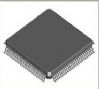
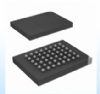
The memory M29DW640D is offered in TSOP48 (12x20mm) and TFBGA63 (7x11mm, 0.8mm pitch) packages. The memory is supplied with all the bits erased (set to 1').

 M29DW640D Data Sheet