Features: Device Architecture
• Design Technology:90nm
• Supply Voltage:1.8V (1.7V ~ 1.95V), 2.65V (2.4 ~ 2.9V), 3.3V (2.7 ~3.6V)
• Host Interface:16 bit
• 3KB Internal BufferRAM:1KB BootRAM, 2KB DataRAM
• SLC NAND Array:(1K+32)B Page Size, (64K+2K)B Block Size
Device Performance
• Host Interface Type:Synchronous Burst Read
- Up to 66MHz clock frequency
- Linear Burst 4-, 8-, 16, 32-words with wrap around
- Continuous 512 word Sequential Burst
Asynchronous Random Read
- 76ns access time
• Programmable Burst Read Latency Latency 3(up to 40MHz), 4, 5, 6, and 7
• Multiple Sector Read:Up to 2 sectors using Sector Count Register
• Multiple Reset Modes:Cold/Warm/Hot/NAND Flash Core Resets
• Multi Block Erase up to 64 Blocks
• Low Power Dissipation:Typical Power,
- Standby current : 10A @1.8V Device
25A @2.65V/3.3V Device
- Synchronous Burst Read current(66MHz) : 15mA@1.8V Device
20mA@2.65V/3.3v Device
- Load current : 30mA@1.8v Device,
30mA@2.65V/3.3V Device
- Program current : 25mA@1.8V Device,
28mA@2.65V/3.3V Device
- Erase current : 20mA@1.8V Device,
23mA@2.65V/3.3V Device
- Multi Block Erase current : 20mA@1.8V Device,
23mA@2.65V/3.3V Device
System Hardware
• Voltage detector generating internal reset signal from Vcc
• Hardware reset input (RP)
• Data Protection Modes
• User-controlled One Time Programmable(OTP) area
• Internal 2bit EDC / 1bit ECC
• Internal Bootloader supports Booting Solution in system
• Handshaking Feature
• Detailed chip information
Synchronous Burst Read
Asynchronous Random Read
- 76ns access time
Asynchronous Random Write
- Write Protection for BootRAM
- Write Protection for NAND Flash Array
- Write Protection during power-up
- Write Protection during power-down
- INT pin indicates Ready / Busy
- Polling the interrupt register status bit
- by ID register
Packaging
• 256Mb products 67ball, 7mm x 9mm x max 1.0mmt , 0.8mm ball pitch FBGA 48 TSOP 1, 12mm x 20mm, 0.5mm pitch
Pinout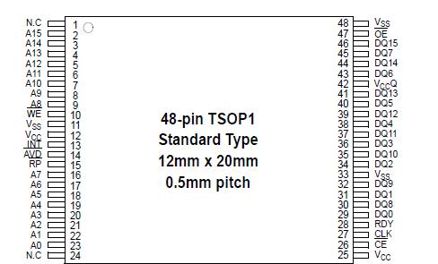 Specifications
|
Parameter |
Symbol |
Rating |
Unit |
| Voltage on any pin relative to VSS |
Vcc |
Vcc (for 1.8V) |
-0.5 to + 2.45 |
V |
|
Vcc (for 2.65V/3.3V) |
-0.5 to + 4.6 |
| All Pins |
VIN (for 1.8V) |
-0.5 to + 2.45 |
|
VIN (for 2.65V/3.3V) |
-0.5 to + 4.6 |
| Temperature Under Bias |
Extended |
Tbias |
-30 to +125 |
°C |
| Industrial |
-40 to +125 |
| Storage Temperature |
Tstg |
-65 to +150 |
°C |
| Short Circuit Output Current |
IOS |
5 |
mA |
| Recommended Operating Temperature |
TA (Extended Temp.) |
-30 to +85 |
°C |
|
TA (Industrial Temp.) |
-40 to +85 |
NOTES:
1. Minimum DC voltage is -0.5V on Input/ Output pins. During transitions, this level should not fall to POR level(typ. 1.5V@1.8V device, 1.8V@2.65V/3.3V device). Maximum DC voltage is Vcc+0.6V on input / output pins which, during transitions, may overshoot to Vcc+2.0V for periods <20ns.
2. Permanent device damage may occur if ABSOLUTE MAXIMUM RATINGS are exceeded. Functional operation should be restricted to the conditions detailed in the operational sections of this data sheet. Exposure to absolute maximum rating conditions for extended periods may affect reliability.
DescriptionThe OneNAND KFG5616x1A-xxB6 is an advanced generation, high-performance NAND-based Flash memory.
KFG5616x1A-xxB6 integrates on-chip a single-level-cell (SLC) NAND Flash Array memory with two independent data buffers, boot RAM buffer, a page buffer for the Flash array, and a one-time-programmable block.
The combination of these memory areas enable high-speed pipelining of reads from host, BufferRAM, Page Buffer, and NAND Flash Array memory.
Clock speeds up to 66MHz with a x16 wide I/O yields a 54MByte/second bandwidth.The OneNAND also includes a Boot RAM and boot loader. This enables the device to efficiently load boot code at device startup from the NAND Array without the need for off-chip boot device.
One block of the NAND Array is set aside as an OTP memory area. This area, available to the user, can be configured and locked with secured user information.
On-chip controller interfaces enable the device to operate in systems without NAND Host controllers.

 KFG5616x1A-xxB6 Data Sheet


