K5D5657DCM-F015

Features: <Common>· Operating Temperature : -25°C ~ 85°C· Package : 107-ball FBGA Type - 10.5x13mm, 0.8mm pitch<NAND>· Power Supply Voltage : 2.4~2.9V· Organization- Memory Cell Array : (32M + 1024K)bit x 8bit- Data Register : (512 + 16)bit x 8bit· Automatic Program and Erase- Page Pro...

product image

K5D5657DCM-F015 Picture
SeekIC No. : 004383113 Detail

K5D5657DCM-F015: Features: <Common>· Operating Temperature : -25°C ~ 85°C· Package : 107-ball FBGA Type - 10.5x13mm, 0.8mm pitch<NAND>· Power Supply Voltage : 2.4~2.9V· Organization- Memory Cell Array : ...

floor Price/Ceiling Price

Part Number:
K5D5657DCM-F015
Supply Ability:
5000

Price Break

  • Qty
  • 1~5000
  • Unit Price
  • Negotiable
  • Processing time
  • 15 Days
Total Cost: $ 0.00

SeekIC Buyer Protection PLUS - newly updated for 2013!

  • Escrow Protection.
  • Guaranteed refunds.
  • Secure payments.
  • Learn more >>

Month Sales

268 Transactions

Rating

evaluate  (4.8 stars)

Upload time: 2024/11/23

Payment Methods

All payment methods are secure and covered by SeekIC Buyer Protection PLUS.

Notice: When you place an order, your payment is made to SeekIC and not to your seller. SeekIC only pays the seller after confirming you have received your order. We will also never share your payment details with your seller.
Product Details

Description


Features:

<Common>
· Operating Temperature : -25°C ~ 85°C
· Package : 107-ball FBGA Type - 10.5x13mm, 0.8mm pitch
<NAND>
· Power Supply Voltage : 2.4~2.9V
· Organization
- Memory Cell Array : (32M + 1024K)bit x 8bit
- Data Register : (512 + 16)bit x 8bit
· Automatic Program and Erase
- Page Program : (512 + 16)Byte
- Block Erase : (16K + 512)Byte
· Page Read Operation
- Page Size : (512 + 16)Byte
- Random Access : 10ms(Max.)
- Serial Page Access : 50ns(Min.)
· Fast Write Cycle Time
- Program time : 200ms(Typ.)
- Block Erase Time : 2ms(Typ.)
· Command/Address/Data Multiplexed I/O Port
· Hardware Data Protection
- Program/Erase Lockout During Power Transitions
· Reliable CMOS Floating-Gate Technology
- Endurance : 100K Program/Erase Cycles
- Data Retention : 10 Years
· Command Register Operation
· Intelligent Copy-Back
· Unique ID for Copyright Protection
<Mobile SDRAM>
· Power Supply Voltage : 1.65~1.95V
• LVCMOS compatible with multiplexed address.
• Four banks operation.
• MRS cycle with address key programs.
-. CAS latency (1, 2 & 3).
-. Burst length (1, 2, 4, 8 & Full page).
-. Burst type (Sequential & Interleave).
• EMRS cycle with address key programs.
• All inputs are sampled at the positive going edge of the system
clock.
• Burst read single-bit write operation.
• Special Function Support.
-. PASR (Partial Array Self Refresh).
-. Internal TCSR (Temperature Compensated Self Refresh)
-. DS (Driver Strength)
• DQM for masking.
• Auto refresh.
• 64ms refresh period (4K cycle).
• Commercial Temperature Operation (-25°C ~ 70°C).


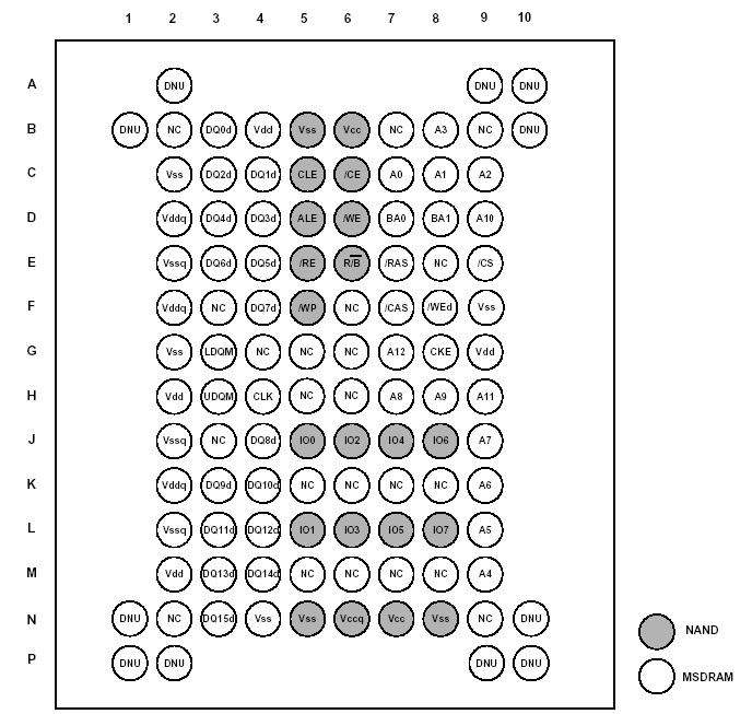
Pinout

  Connection Diagram


Specifications

Rating Symbol Rating Unit
Voltage on any pin relative to VSS VIN/OUT -0.6 to + 4.6 V
VCC -0.6 to + 4.6 V
VCCQ -0.6 to + 4.6 V
Temperature Under Bias TBIAS -40 to +125 °C
Storage Temperature TSTG -65 to +150 °C
Short Circuit Current Ios 5 mA


Description

The K5D5657DCM is a Multi Chip Package Memory which combines 256Mbit Nand Flash Memory and 256Mbit synchronous high data rate Dynamic RAM.

256Mbit NAND Flash memory K5D5657DCM-F015 is organized as 32M x8 bits and 256Mbit SDRAM is organized as 4M x16 bits x4 banks. In 256Mbit NAND Flash, a 528-Byte page program can be typically achieved within 200us and an 16K-Byte block erase can be typically achieved within 2ms. In serial read operation, a byte can be read by 50ns. DQ pins serve as the ports for address and data input/output as well as command inputs. Even the write-intensive systems can take advantage of FLASH¢s extended reliability of 100K program/erase cycles with real time mapping-out algorithm. These algorithms have been implemented in many mass storage applications.

In 256Mbit SDRAM, Synchronous design make a device controlled precisely with the use of system clock and I/O transactions are possible on every clock cycle. Range of operating frequencies, programmable burst length and programmable latencies allow the same device to be useful for a variety of high bandwidth, high performance memory system applications.

The K5D5657DCM-F015 is suitable for use in data memory of mobile communication system to reduce not only mount area but also power consumption. This K5D5657DCM-F015 is available in 107-ball FBGA Type.


Customers Who Bought This Item Also Bought

Margin,quality,low-cost products with low minimum orders. Secure your online payments with SeekIC Buyer Protection.
Static Control, ESD, Clean Room Products
Inductors, Coils, Chokes
Crystals and Oscillators
Discrete Semiconductor Products
Programmers, Development Systems
View more