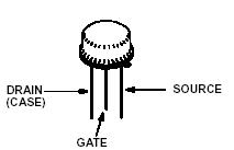
Features: • 3.5A, 400V
•
rDS(ON) = 1.000Ω
• Single Pulse Avalanche Energy Rated
• SOA is Power Dissipation Limited
• Nanosecond Switching Speeds
• Linear Transfer Characteristics
• High Input Impedance
• Related Literature
- TB334 "Guidelines for Soldering Surface Mount Components to PC Boards"
Pinout Specifications IRFF330 UNITS
Drain to Source Voltage (Note 1) . . . . . . . . . . . . . . . . . . . . . . . . . . .VDS 400 V
Drain to Gate Voltage (RGS = 20kΩ) (Note 1) . . . . . . . . . . . . . . . . VDGR 400 V
Continuous Drain Current . . . . . . . . . . . . . . . . . . . . . . . . . . . . . . . . . ID 3.5 A
Pulsed Drain Current (Note 3) . . . . . . . . . . . . . . . . . . . . . . . . . . . . . IDM 14 A
Gate to Source Voltage . . . . . . . . . . . . . . . . . . . . . . . . . . . . . . . . . ..VGS ±20 V
Maximum Power Dissipation . . . . . . . . . . . . . . . . . . . . . . . . . . . . . . ..PD 25 W
Linear Derating Factor . . . . . . . . . . . . . . . . . . . . . . . . . . . . . . . . . . . . . . . . . . .. 0.2 W/
Single Pulse Avalanche Energy Rating (Note 4) . . . . . . . . . . . . EAS 300 mJ
Operating and Storage Temperature Range . . . . . . . . . . . . . . . TJ, TSTG -55 to 150
Maximum Temperature for Soldering
Leads at 0.063in (1.6mm) from Case for 10s. . . . . . . . . . . . . . . . . . . TL 300
Package Body for 10s, See Techbrief 334 . . . . . . . . . . . . . . . . . . .. Tpkg 260
Description This N-Channel enhancement mode silicon gate power field effect transistor IRFF330 is an advanced power MOSFET designed, tested, and guaranteed to withstand a specified level of energy in the breakdown avalanche mode of operation. All of these power MOSFETs are designed for applications such as switching regulators, switching convertors, motor drivers, relay drivers, and drivers for high power bipolar switching transistors requiring high speed and low gate drive power. These types can be operated directly from integrated circuits.
Formerly developmental type IRFF330.

 IRFF330 Data Sheet


