ILD615

Features: • Identical Channel to Channel Footprint• Dual and Quad Packages Feature:- Reduced Board Space- Lower Pin and Parts Count- Better Channel to Channel CTR Match- Improved Common Mode Rejection• Isolation Test Voltage from Double Molded Package, 5300 VRMS• Lead-free ...

product image

ILD615 Picture
SeekIC No. : 004374231 Detail

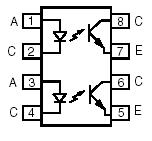
ILD615: Features: • Identical Channel to Channel Footprint• Dual and Quad Packages Feature:- Reduced Board Space- Lower Pin and Parts Count- Better Channel to Channel CTR Match- Improved Common ...

floor Price/Ceiling Price

Part Number:
ILD615
Supply Ability:
5000

Price Break

  • Qty
  • 1~5000
  • Unit Price
  • Negotiable
  • Processing time
  • 15 Days
Total Cost: $ 0.00

SeekIC Buyer Protection PLUS - newly updated for 2013!

  • Escrow Protection.
  • Guaranteed refunds.
  • Secure payments.
  • Learn more >>

Month Sales

268 Transactions

Rating

evaluate  (4.8 stars)

Upload time: 2024/5/28

Payment Methods

All payment methods are secure and covered by SeekIC Buyer Protection PLUS.

Notice: When you place an order, your payment is made to SeekIC and not to your seller. SeekIC only pays the seller after confirming you have received your order. We will also never share your payment details with your seller.
Product Details

Description


Features:

• Identical Channel to Channel Footprint
• Dual and Quad Packages Feature:
- Reduced Board Space
- Lower Pin and Parts Count
- Better Channel to Channel CTR Match
- Improved Common Mode Rejection
• Isolation Test Voltage from Double Molded Package, 5300 VRMS
• Lead-free component
• Component in accordance to RoHS 2002/95/EC and WEEE 2002/96/EC


Application

• UL1577, File No. E52744 System Code H or J, Double Protection
• CSA 93751
• BSI IEC60950 IEC60965
• DIN EN 60747-5-2 (VDE0884) DIN EN 60747-5-5 pending Available with Option 1


Pinout

  Connection Diagram


Specifications

Tamb = 25 °C, unless otherwise specified Stresses in excess of the absolute Maximum Ratings can cause permanent damage to the device. Functional operation of the device is not implied at these or any other conditions in excess of those given in the operational sections of this document. Exposure to absolute Maximum Rating for extended periods of the time can adversely affect reliability.
Parameter Test condition Symbol Value Unit
Reverse voltage   VR 6.0 V
Forward current   IF 60 mA
Surge current   IFSM 1.5 A
Power dissipation   Pdiss 100 mW
Derate linearly from 25 °C     1.33 mW/°C


Description

The ILD615 are multi-channel phototransistor optocouplers that use GaAs IRLED emitters and high gain NPN phototransistors. These devices are constructed using over/under leadframe optical coupling and double molded insulation technology resulting a withstand test voltage of 7500 VACPEAK and a working voltage of 1700 VRMS.

The binned min./max. and linear CTR characteristics make these devices well suited for DC or AC voltage detection. Eliminating the phototransistor base connection provides added electrical noise immunity from the transients found in many industrial control environments.

Because of guaranteed maximum non-saturated and saturated switching characteristics, the ILD615 can be used in medium speed data I/O and control systems. The binned min./max. CTR specification allow easy worst case interface calculations for both level detection and switching applications. Interfacing with a CMOS logic is enhanced by the guaranteed CTR at IF = 1.0 mA.


Customers Who Bought This Item Also Bought

Margin,quality,low-cost products with low minimum orders. Secure your online payments with SeekIC Buyer Protection.
Inductors, Coils, Chokes
Test Equipment
Resistors
LED Products
Semiconductor Modules
View more